In general isolated power supplies, optocoupler isolation feedback is a simple, low-cost way. However, for the various connection methods of optocoupler feedback and their differences, no in-depth research has been seen yet. Moreover, in many occasions, because the understanding of the working principle of the optocoupler is not deep enough, the optocoupler connection method is confusing, which often causes the circuit to fail to work normally. This study will analyze the working principle of optocoupler in detail, and compare several typical methods of optocoupler feedback. 1. Common connection methods and working principles The optocoupler models commonly used for feedback are TLP521 and PC817. Here, the TLP521 is taken as an example to introduce the characteristics of such an optocoupler. The primary side of the TLP521 is equivalent to a light-emitting diode. The larger the primary current If, the stronger the light intensity, and the larger the current Ic of the secondary transistor. The ratio of the secondary triode current Ic to the primary diode current If is called the current amplification factor of the optocoupler, which varies with temperature and is greatly affected by temperature. The optocoupler used for feedback uses the "primary current change will cause the secondary side current to change" to achieve feedback. Therefore, in the case of severe changes in ambient temperature, since the temperature drift of the amplification factor is relatively large, it should be achieved without optocoupler. Feedback. In addition, the use of such optocouplers must pay attention to the design of peripheral parameters, so that it works in a relatively wide linear band, otherwise the circuit is too sensitive to operating parameters, which is not conducive to the stable operation of the circuit. Feedback is usually selected in conjunction with TLP521. At this time, the working principle of the TL431 is equivalent to a voltage error amplifier with an internal reference of 2.5V, so between the 1st and 3rd feet, the compensation network should be connected. TL431 is the role of optocoupler in three-terminal programmable shunt regulator diode switching power supply
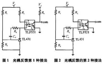
The common optocoupler feedback is the first connection, as shown in Figure 1. In the figure, Vo is the output voltage and Vd is the supply voltage of the chip. The com signal is connected to the error amplifier output pin of the chip, or the internal voltage error amplifier of the PWM chip (such as UC3525) is connected to the non-inverting amplifier form, and the com signal is connected to its corresponding non-inverting terminal pin. Note that the ground on the left is the output voltage ground, and the ground on the right is the power supply voltage of the chip. The two are isolated by optocouplers. The operation of the connection shown in Figure 1 is as follows: When the output voltage rises, the voltage of pin 1 of the TL431 (corresponding to the inverting input of the voltage error amplifier) ​​rises, and the voltage of pin 3 (corresponding to the output pin of the voltage error amplifier) Decrease, the primary current If of the optocoupler TLP521 increases, the output current Ic of the other end of the optocoupler increases, the voltage drop across the resistor R4 increases, the com pin voltage decreases, the duty cycle decreases, and the output voltage decreases; Conversely, when the output voltage is reduced, the adjustment process is similar. The second type of connection is common in the role of optocouplers in switching power supplies, as shown in Figure 2. Different from the first connection method, the fourth pin of the optocoupler in the connection is directly connected to the error amplifier output end of the chip, and the voltage error amplifier inside the chip must be connected to the non-inverting terminal potential higher than the inverting terminal potential. The form, using one of the characteristics of the op amp - when the output current of the op amp is too large (beyond the op amp current output capability), the output voltage value of the op amp will decrease, and the larger the output current, the more the output voltage drops. Therefore, in this circuit, the two input pins of the error amplifier of the PWM chip must be connected to a fixed potential, and the potential of the same terminal should be higher than the potential of the opposite terminal to make the initial output voltage of the error amplifier. High. The working principle of the connection method shown in Figure 2 is: when the output voltage rises, the primary current If increases, and the output current Ic increases. Since Ic has exceeded the current output capability of the voltage error amplifier, the com pin voltage drops. The air ratio is reduced and the output voltage is decreased; conversely, when the output voltage is decreased, the adjustment process is similar.
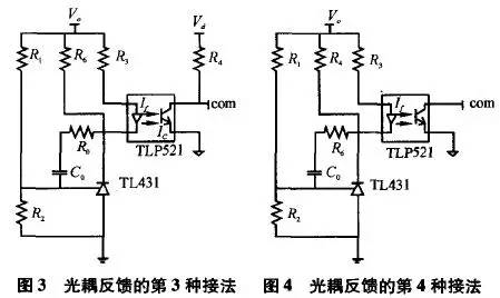
A common fourth connection is shown in Figure 4. The connection method is similar to the second connection method. The difference is that a resistor R4 is connected between the com terminal and the photocoupler pin 4, and its function is consistent with R6 in the third connection method, and the working principle is basically the same. 2.
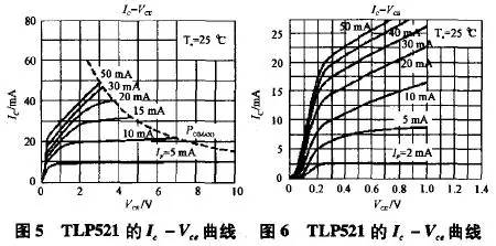
2. Comparison of various connections Before the comparison, several characteristic curves of the actual optocoupler TLP521 need to be analyzed. The first is the Ic-Vce curve, as shown in Figure 5 and Figure 6. The role of optocoupler in switching power supply
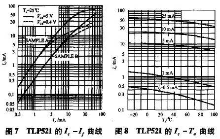
As can be seen from Fig. 8, when If is greater than 5 mA, the Ic-Ta curves are substantially parallel to each other.
Based on the above analysis, the following is a comparison of the characteristics and the scope of application for different typical connections. This study uses an actual isolated half-bridge auxiliary power supply and a flyback power supply as an example. In the first connection method, the voltage connected to the output terminal of the voltage error amplifier is obtained after the external voltage is stepped down by the resistor R4, and is not affected by the current output capability of the voltage error amplifier. The working point of the optocoupler can be adjusted freely through its external resistor. According to the previous analysis, the static working point value of the current If is about 10 mA, and the corresponding optocoupler operating temperature is changed from 0 to 100 ° C, and the value is between 20 and 15 mA. Generally, the amplitude of the triangular wave of the PWM chip does not exceed 3V. Therefore, the size of the selected resistor R4 is 670Ω, and at the same time, the static working point value of the 3-pin voltage of the TL431 is determined to be 12V, then the value of the resistor R3 can be selected to be 560Ω. The values ​​of the resistors R1 and R2 are easily selected, and are taken here as 27k and 4.7k. Resistor R5 and capacitor C1 are PI compensated, here taken as 3k and 10nF. In the experiment, the half-bridge auxiliary power output load is the various control chips on the control board, plus the dead load of each of the multiple outputs, the final actual power is about 30w. The actual measured optocoupler 4 pin voltage (this voltage is compared with the chip triangle wave to determine the drive duty cycle) waveform, as shown in Figure 9. The corresponding drive signal waveform is shown in Figure 10. The driving waveform of Fig. 10 has a negative voltage portion because the driving of the upper and lower tubes is wound around a driving magnetic ring. It can be seen that the duty cycle of the drive signal is relatively large, about 0.7.
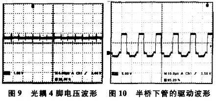
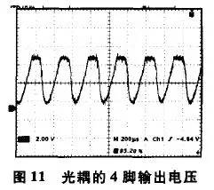
Similarly, for the above half-bridge auxiliary power supply circuit, the connection method 2 is used instead of the connection method 1, the closed-loop is unstable, and the voltage waveform of the photocoupler 4 pin is observed by an oscilloscope, and there is obvious oscillation. The 4-pin output voltage of the optocoupler (corresponding to the error amplifier output pin voltage of the UC3525), the waveform is shown in Figure 11, and significant oscillations can be found. This is because the steady-state duty ratio of this half-bridge power supply is relatively large. When the connection method is 2, the optocoupler gain is large, and the system is unstable and oscillates.
In fact, the second type of connection is more common in the flyback circuit. This is because the flyback circuit is generally considered for efficiency. The circuit usually works in the discontinuous mode, and the driving duty ratio is relatively small. The corresponding optocoupler current Ic is compared. Large, referring to the above analysis, the closed loop is also relatively easy to stabilize.
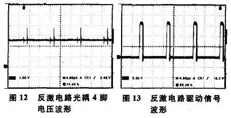
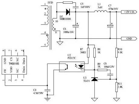
The following is another experimental flyback circuit that works in discontinuous mode and actually measures the voltage waveform of its optocoupler 4 pin, as shown in Figure 12. The actual measured drive signal waveform, as shown in Figure 13, has a duty cycle of approximately 0.2.
Therefore, in the optocoupler feedback design, in addition to setting its peripheral parameters according to the characteristic parameters of the optocoupler, it should also be known that the selection of the feedback mode at different duty cycles is also limited. Feedback modes 1, 3 are suitable for any duty cycle, and feedback modes 2, 4 are more suitable for use in situations where the duty cycle is relatively small. 3. Conclusion This study lists four typical optocoupler feedback connections, analyzes the principle of optocoupler feedback under various connections and various limiting factors, and compares the different points of various connections. Through the actual half-bridge and flyback circuit test, the limitation of the duty cycle of the circuit operation to the feedback mode selection is verified. Finally, the optocoupler feedback is summarized, which has certain reference value for future optocoupler feedback design. The optocoupler of the switching power supply is mainly isolated, providing feedback signals and switching functions. The power supply of the optocoupler in the switching power supply circuit is supplied from the secondary voltage of the high-frequency transformer. When the output voltage is lower than the voltage of the Zener diode, the signal optocoupler is turned on, and the duty ratio is increased to increase the output voltage; Turning off the optocoupler reduces the duty cycle, causing the output voltage to decrease. When the secondary load of the high-frequency transformer is overloaded or the switch circuit is faulty, there is no optocoupler power supply. The optocoupler controls the switch circuit to not start, thus protecting the switch tube from being broken down and burned.
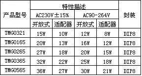
Usually the optocoupler is used with the TL431. The following are some of the circuits of the LED power driver chip (switching power supply chip) TMG0321/TMG0165/TMG0265/TMG03655. The two resistors are sampled in series to the 431R terminal for comparison with an internal comparator. Then, according to the compared signal, the resistance of the 431K terminal (the anode is connected to the photocoupler) to ground is controlled, and then the brightness of the internal LED of the optocoupler is controlled. (The inside of the optocoupler is a light-emitting diode, and one side is a phototransistor) through the intensity of the light. Controlling the resistance of the CE terminal of the other end transistor is also changing the current of the LED power supply driving chip (switching power supply chip) TMG0321/TMG0165/TMG0265/TMG0365 detecting pin (1 pin: voltage feedback pin, adjusting the optical coupling to the ground to adjust Control ratio). According to the current, the LED power supply driver chip (switching power supply chip) TMG0321/TMG0165/TMG0265/TMG0365 will automatically adjust the duty cycle of the output signal to achieve the purpose of voltage regulation.
The TMG0321/TMG0165/TMG0265/TMG0365 chip is a highly integrated, high performance PWM+MOSFET tube 2-in-1 current-mode off-line switching power supply controller. Suitable for all kinds of low-power switching power supplies such as chargers, power adapters, LED drive power supplies, etc. With DIP8 package, it can output 0~36W without adding heat sink (plus heat can make it bigger). The circuit structure is simple and the cost is low. It has perfect protection functions including overvoltage, undervoltage, overtemperature, overload and short circuit protection. Fixed oscillation frequency and frequency hopping function can reduce EMI. The standby power is low, and it enters the skip cycle mode during standby, which meets the requirements of the “Energy Star†waiting machine power consumption standard.
The photoelectric switch is the abbreviation of the photoelectric proximity switch. It utilizes the shielding or reflection of the light beam by the detected object, and the circuit is connected by the synchronization loop to detect the presence of the object. The object is not limited to metal, all objects that can reflect light (or block light) can be detected.
Photoelectric Proximity Sensor,Photoelectric Switch Sensor,Photoelectric Proximity Switch,Infrared Photoelectric Switch Sensor
Changchun Guangxing Sensing Technology Co.LTD , https://www.gx-encoder.com