This design uses LED1, LED2, LED3 lamp and button S1 as peripherals. The P10, P11, and P14 ports are used as output ports to drive LED1/LED2/LED3. The P01 port is an input port and accepts button signal input (high level is a button signal).
1. High performance 2.4G RF module Q2530RF
Q2530RF is based on TI's second generation 2.4GHz IEEE 802.15.4 /
RF4CE/ZigBee's second-generation system-on-chip solution CC2530 F256's full-featured module integrates RF transceiver and MCU control functions. The peripheral components include a 32MHz crystal oscillator and a 32.768KHz crystal oscillator and some other resistive components. The RF part adopts balun matching and external high-gain SMA antenna, which has high receiving sensitivity and long transmission distance. The maximum transmission distance of open environment can reach 400 meters. The module leads all IO ports of the CC2530 for functional evaluation and secondary development.
2. Multi-function development board Q2530EB
Multi-function expansion board Q2530EB can support a variety of RF main control modules (such as Q2530RF, etc.), with serial port LCD display interface, USB power supply interface, DC 5V power interface, battery interface, RS232 interface, DEBUG interface, five-way button and indicator , infrared remote control signal receiving / transmitting and other modules.
All peripherals are connected to the RF module Q2530RF via interfaces such as SPI bus/UART/DEBUG and are fully controlled and accessed by the Q2530RF.
Multi-function simulation expansion board Q2530EB adopts three power supply modes: DC 5V power supply, USB interface power supply, battery power supply, jumper selection can be set in socket P5, PIN1-PIN2 is battery power supply, PIN2-PIN3 is external DC power supply or USB interface powered by. The power switch is P4.
The battery compartment on the back of the Q2530EB board can hold three 5th dry batteries, the output voltage is 3.4~4.5V, and the onboard power supply circuit adjusts it to +3.3V stable DC voltage output for later use. When the battery voltage is lower than 3.4V, the battery should be replaced to keep the module working properly.
The Q2530EB has a DC 5V power adapter interface P2 and a USB interface P1. The input voltage is stepped down by the regulator to +3.3V output for use by the rear pole.
The Q2530EB LCD module provides serial port control. The LCD module is placed on the odd side of the P12, and the 1~16 pin corresponds to the P~1~31 pin. Unlike the TI official SmartRF05EB, our multi-function simulation expansion board Q2530EB LCD The module is an optional component, and a 128*64 dot matrix graphic liquid crystal display module is selected, and the driving source code of the liquid crystal module is provided. For project developers who don't want to waste energy in this process, we have prepared the LCD driver files for TI platform such as Z-Stack/Basic RF. You only need to put TI documents in this file. Replace the file with the same name in it.
The RS232 interface of the multi-function emulation expansion board Q2530EB can be used to communicate with other peripherals. U5 is used for RS232 level conversion on the circuit. Connect to the peripheral via the RS232 socket P10.
The serial port is provided with a power jumper P9 for setting the serial port chip to start and stop.
The serial port has two transceiver indicators D5 and D6, which are used to indicate whether the serial port receives or is transmitting data, and D7 is the serial port power indicator.
The main control part of the multi-function simulation expansion board Q2530EB is an external RF control module. Connect to the Q2530RF control module via P14, P15.
The multi-function simulation expansion board Q2530EB provides the DEBUG interface P13 to be connected to the emulator, and the related signals (SPI bus, DEBUG signal, etc.) are connected to the RF control module Q2530RF through the sockets P14 and P15. These signal lines can also be disconnected through P11.
The multi-function simulation expansion board Q2530EB provides a 5-phase button (U3), four touch buttons (S1/S2/S3/S4), and six LEDs (D1/D2/D3/D4/D8/D9).
U3 can detect five directions (center, up, down, left, right) and one button action. In this case, there are five signals of KEY_UP, KEY_DOWN, KEY_LEFT, KEY_RIGHT, and KEY_PUSH to describe the direction button action. If you use five AD ports to sample the signal, it is unrealistic or uneconomical for some RF control modules. When paired with the RF control module Q2530RF, the Q2530EB provides two signals KEY_MOVE, KEY_LEVEL to describe the button action. KEY_MOVE is high when the button is moved in any direction or pressed.
At the same time, the value of another signal KEY_LEVEL represents the direction of the button.
Among the four touch buttons (S1/S2/S3/S4), S4 is the system reset button (RESET), S3 is the RemoTI development system definition button, and S1 and S2 are Zigbee development system definition buttons.
Among the six LEDs (D1/D2/D3/D4/D8/D9), D1/D2/D3/D4 defines the LED for the Zigbee development system, and D8/D9 defines the LED display for the RemoTI development system.
The multi-function expansion development board Q2530EB is equipped with a serial port FLASH (U7) for data and parameter storage.
The input of the infrared remote control signal is completed by U8 and other resistance-receiving components. The IR signal is demodulated to the carrier and then input to the RF control module Q2530RF. The output of the infrared remote control signal is directly driven by the RF control module Q2530RF to transmit the infrared emitting diode D10.
The board contains a 10k potentiometer, which is convenient for users to learn and experiment with analog A/D sampling. The jumper connection between potentiometer and 2530 is disconnected by default. Before the experiment, the 25 and 26 legs of P16 should be jumped. The wire cap is shorted; since the three pins of the potentiometer, the liquid crystal backlight, and the standby LED are multiplexed with the same pin of the 2530, the 31 and 32 pins of the P11 and the 27 and 28 pins of the P16 should also be disconnected during use.
3. Multi-function battery board Q2530BB
The Q2530BB's RF control board interface definition is consistent with the Q2530EB board.
Continue the Q2530EB three power supply modes: DC5V, USB or battery powered. Jumper selection can be set at outlet P5, PIN1-PIN2 for battery power, and PIN2-PIN3 for external DC power or USB. The power switch is P4, and the switch has an “ONâ€/“OFF†character indication.
The Q2530BB provides the DEBUG interface P10 connected to the emulator. The related signals (SPI bus, DEBUG signal, etc.) are connected to the RF control module Q2530RF through the sockets P8 and P9, and the related signals can be connected and disconnected through P11.
The user can debug and download the program of the RF control module Q2530RF through the emulator on the PC.
The Q2530BB also provides the ability to implement the protocol analyzer Packet Sniffer in conjunction with the emulator.
The Q2530BB provides one touch button S2 and one reset button S1. Two LED indicators D1 and D2 are also available.
Q2530BB uses a photoresistor to form the illuminance sensor circuit, a temperature sensor circuit composed of a temperature sensitive resistor, and then input the IC for AD conversion. The development system provides a sample program for sampling two external sensor voltages when the zstack is networked.
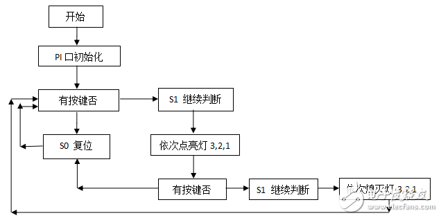
The following is a flow chart of this design:
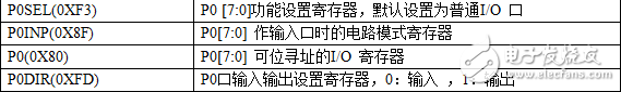
Design related registers: P1, P1DIR, P0SEL, P0INP, P0, P0DIR
Program function : This design program realizes the button control LED light: the power-on button once, LED3, LED2, LED1 light up in turn; once again, LED3, LED2, LED1 are extinguished in turn;
The program code for this internship is as follows:
//BY QIUJIE TECH.INC
#include 《ioCC2530.h》
#define uint unsigned int
#define uchar unsigned char
/ / Define the port of the control light
#define RLED P1_0 //Define LED1 as P10 port control
#define GLED P1_1 //Define LED2 as P11 port control
#define YLED P1_4 //Define LED3 as P14 port control
#define KEY1 P0_1 //Define the button as P01 port control
/ / Function statement
Void Delay(uint); //Delay function declaration
Void InitIO(void); //Initialize function declaration
Void InitKey(void); //Initialize button function declaration
Uchar KeyScan(void); //Key scan function declaration
Uchar Keyvalue = 0; //Define the variable record button action
Uint KeyTouchtimes = 0 ; //Define the number of key record keystrokes
/****************************
//Key initialization
*****************************/
Void InitKey(void)
{
P0SEL &= ~0X02;
P0DIR &= ~0X02; //The button is at P01 and set to input mode.
P0INP |= 0x02; //Upload
}
/****************************
/ / Initialize the program, define P10, P11, P14 as the output port, and initialize the LED light to off
*****************************/
Void InitIO(void)
{
P1DIR |= 0x13; //P10, P11, P14 are defined as outputs
RLED = 0;
GLED = 0;
YLED = 0; //LED light is initialized to off
}
/*****************************************
/ / button action record function
*****************************************/
Uchar KeyScan(void)
{
If(KEY1 == 1) //Active high
{
Delay (100); / / detected button
If(KEY1 == 1)
{
While(KEY1); //until the button is released
Return(1);
}
}
Return(0);
}
/***************************
/ / Main function
***************************/
Void main(void)
{
InitIO (); / / Initialize the LED light control IO port
InitKey (); / / initialization button control IO port
While(1)
{
Keyvalue = KeyScan(); //Read button action
If(Keyvalue == 1) //Press the button to set it to LED3, LED2, LED1 flashing in reverse order
{
GLED = ! GLED;
Delay (20000);
YLED = ! YLED;
Delay (20000);
RLED = ! RLED;
Delay (20000);
}
}
}
The following is the schematic of this design
Q2530BB battery board schematic
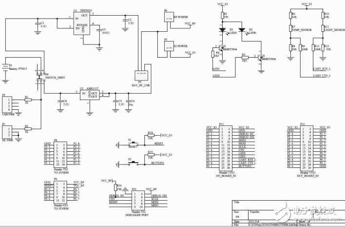
Q2530EB development board schematic
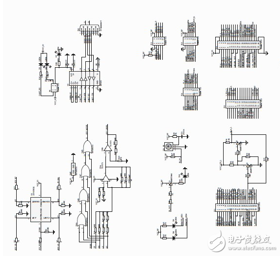
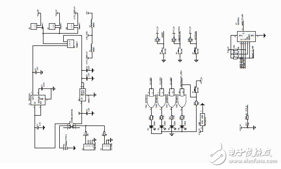
Q2530RF RF board schematic

Self-healing Hydrogel Screen Protector
The Screen Protector has a self-healing technology that can automatically eliminate small scratches on the Protective Film within 24 hours. Significantly reduce dust, oil stains and fingerprint smudges, anti-scratch.
The Screen Protection Film is very suitable for curved or flat screens. The Soft Hydrogel Film perfectly matches the contour of your device. Will not affect any functions of the phone.
The Ultra-Thin Protective Film with a thickness of only 0.14mm uses 100% touch screen adaptive screen touch screen technology, complete touch screen response, high-tech technology makes the screen touch to achieve zero delay, ultra-thin material brings you "realism".
The Protection Film has excellent clarity and incredible toughness, providing a high level of clarity and a glass-like surface, highlighting the sharpness of the most advanced smartphone display images and bright colors.
If you want to know more about Self Repair Screen Protector products, please click the product details to view the parameters, models, pictures, prices and other information about Self Repair Screen Protector.
Whether you are a group or an individual, we will try our best to provide you with accurate and comprehensive information about the Self Repair Screen Protector!
Self-healing Protective Film, Self-repairing Screen Protector,Self-healing Screen Protector, Self-Healing Hydrogel Film,Hydrogel Film Screen Protector
Shenzhen Jianjiantong Technology Co., Ltd. , https://www.jjtscreenprotector.com