[Foreword] According to the importance of the various measures taken in the design of electromagnetic compatibility products, the design is divided into several levels, and comprehensive analysis is carried out to make appropriate adjustments until perfection. This is the electromagnetic stratification layer proposed in this paper. Comprehensive design method." The electromagnetic compatibility test can be successfully performed once.
When people develop new products, they are often eager to realize the functions of the products. Therefore, they use the experience of low frequency and low speed, and are satisfied with the use of software to connect the single chip, chip and components. It is hoped that the product function, performance and performance will be realized. Not only is it at a low level, but it also delays precious time.
In fact, with the increase of the integrated circuit clock rate, the increase of the rising and falling edge rate, the reduction of the power supply voltage, the increase of product complexity and density, and the shortening of the design cycle, the experience of using low frequency and low speed has completely failed to realize the product. Features, performance and performance. If you redesign at the end of the product design, the cost is high. If the date is delayed, the loss is even greater.
Therefore, the design goal of “launching products in the first place†is a vital need for competition. To achieve product specification functions in the first place, to maximize product performance and achieve maximum performance, EMC design must be done. In order to solve the EMC problem at the lowest cost, it is necessary to design the EMC at the same time as the functional design and select the correct method.
Now, the focus of product design has shifted from functional design and logic design to EMC design.
The correct method for electromagnetic compatibility design should be done: treating both the symptoms and the root causes, and focusing on the root cause. It is from the source of governance electromagnetic compatibility problems, according to the importance of the order, divided into several levels for design, and comprehensive analysis, make appropriate adjustments until perfect:
The first layer is one of the key things: the selection of active devices and printed circuit board design
The second layer is the second in the root of the problem: grounding design
The third layer is one of the symptoms and treatments: structure / shielding design
The fourth layer is the second part of the problem: the filter design
The fifth layer is the third of the symptoms and treatment: transient disturbance suppression design
The sixth layer is system-level electromagnetic compatibility design
And comprehensive design and software anti-harassment design for grounding, shielding and filtering at each layer. This is called "electromagnetic compatibility layering and comprehensive design method." The electromagnetic compatibility test can be successfully performed once.
"Electromagnetic compatibility stratification and comprehensive design method" was first proposed by the author in the "National Electromagnetic Compatibility Standards and Quality Certification Seminar" in May 2000, and has been published for more than ten years. Since its promotion in the country for more than ten years, a group of enterprises have stepped out of the "weird circle" that the "test and modification method" has caused the failure of the electromagnetic compatibility test, so that the electromagnetic compatibility design is actively carried out at the beginning of product design. Moreover, the investment in electromagnetic compatibility design only needs 1% (usually 5% to 10% in China). It reduces costs and shortens development time. At the same time, it has also made the "electromagnetic compatibility stratification and comprehensive design method" more substantial and perfect, and has been recognized by many enterprises and units throughout the country.
First-layer active device selection and printed circuit board design
At the source of electromagnetic compatibility problems, to fundamentally solve the EMC problem, the chip selection and printed circuit board design must be done first.
one. Sensitivity and emission characteristics of active devices
Electromagnetic sensitivity characteristics
The in-band sensitivity characteristics of analog devices depend on sensitivity and bandwidth; the out-of-band sensitivity characteristics are expressed in terms of out-of-band rejection.
The in-band sensitivity characteristics of logic devices depend on noise margin or noise immunity, and the out-of-band sensitivity characteristics are also represented by out-of-band rejection characteristics.
2. Electromagnetic emission characteristics
Logic devices are the most common source of broadband disturbances with strong harassment emissions. The shorter the rise time tr of the clock waveform, the wider the bandwidth occupied by the corresponding logic pulse
BW=1/ptr
This bandwidth is also the highest frequency component. The actual radiation frequency range may be more than ten times that of BW. Typical values ​​for tr can be found in the device manual.
It is generally believed that the key issue to be considered in PCB design is the clock frequency. In fact, the rise time tr of the clock waveform is the most critical factor. The rise time tr is defined as the time required to rise from 10% of the waveform to 90%. If a square wave is input at one end of the interconnect and a square wave is required at the other end, the interconnect must not only transmit the fundamental of the square wave, but must also transmit all higher harmonics, at least 15 harmonics. wave. That is to say, the clock frequency of the PCB is not important, and the rise time tr and the harmonics that need to be regenerated are the most important. The term describing this requirement is the bandwidth BW, which is the highest frequency component.
3. â–³I noise current, transient load current IL generation and harm
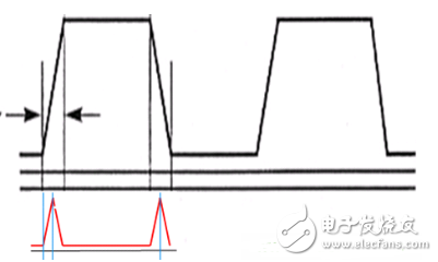
When the digital integrated circuit is powered up, its internal gate circuit will change "0" and "1", that is, the switching state. During the conversion process, the transistors in the gate circuit will be switched between on and off states, and there will be a transient current-inrush current di/dt flowing from the connected power supply entry circuit or from the gate circuit to the ground. This change current is the initial source of ΔI noise, called ΔI noise current. As shown in Figure 1.
Figure 1 â–³I noise current
The sum of the drive line to ground capacitance and the drive gate input capacitance is the load capacitance Cs, which is normally charged, and its value is the power supply voltage. The drive gate is discharged from a high potential to a low potential, and the discharge current is called a transient load current:
IL = Cs&TImes;dv/dt
When the transient load current IL is combined with the ΔI noise current, a stronger electromagnetic disturbance emission is generated. It is the main reason that hinders the realization of the product's prescribed functions and makes the product's performance not fully utilized. Due to the certain lead inductance L on the PCB, the signal line, the power line and the ground line, the instantaneous change current di/dt generated by the combination of the transient load current IL and the ΔI noise current will pass the inductance of the lead inductance L. Peak voltage
V= - Ldi/dt
That is, the ΔI noise voltage, called the Simultaneous Switch Noise SSN, as shown in FIG. 2, causes ground potential and power supply voltage fluctuations (Ground/Power Bounce) to generate electromagnetic disturbance emissions. Therefore, the lead inductance L is one of the root causes of conducted disturbance and radiation disturbance.
Figure 2 spike voltage
Another source of electromagnetic disturbance emission is the source impedance of the equivalent voltage source, that is, the input impedance Z of the power distribution system. The system requires the peak voltage to be within ±2.5% to ±5% of the normal power supply voltage. Equivalent to the source impedance Z to be low enough
V= Z&TImes;ΔI
Regardless of how ΔI changes, the V change is kept small. This can be achieved by installing a decoupling capacitor.
The source impedance Z of the ideal power supply is zero and the potential at any point on the power plane remains constant.
4. Master IC design and packaging characteristics to suppress EMI
IC packaging is also one of the causes of electromagnetic disturbances. The IC package includes a chip, an internal PCB, and a pad. Directly affect the capacitance and inductance of the IC package.
The chip exists as part of the system, and the silicon chip must be packaged and soldered to the PCB. This interconnect, the chip is connected to the PCB via a package, is itself a complex system.
Chip design, packaging, and printed circuit boards should be considered as a system. To ensure that the desired results are obtained after final assembly and power up. The best way to do this is to design, analyze, and validate all of them in parallel.
The package refers to the outer casing for mounting the semiconductor integrated circuit chip, which not only functions to place, fix, seal, protect the chip and enhance the electrothermal performance, but also bridges the internal world and the external circuit of the chip - the wire for the contact on the chip Connect to the pins of the package housing, which in turn connect to other devices through the wires on the printed board. An important indicator to measure the advancement of a chip packaging technology is the ratio of chip area to package area. The closer the ratio is to 1, the smaller the lead inductance. Packaging technology has undergone several generations of changes:
1) Through-hole Package
DIP (Dual In-line Package) Dual in-line package: packaged in the 1970s, with a maximum of 64 pins. The chip area/package area is 1:8.6, which is far from 1 phase, indicating that the package efficiency is very low, the lead wire is long, and the lead inductance is large;
PGA (Pin Grid Array) pin grid array package, pin center distance is 2.54mm, pin count is 64-447. The surface mount PGA pin has a center-to-center distance of 1.27mm and a pin count of 250-528. The lead inductance is large;
2) Surface Mounted Package
In the 1980s, chip carrier packages appeared, including ceramic leadless chip carrier package LCCC, plastic lead chip carrier package PLCC, small outline package SOP (Small Outline Package), and plastic four-sided lead-out package PQFP. The chip area/package area is 1:7.8, and the lead inductance is still large;
3) BGA package and CSP package
With the advancement of integration technology and the use of deep sub-micron technology in the 1990s, LSI, VLSI, and ULSI have emerged, chip integration has been continuously improved, packaging requirements have become stricter, I/O pin counts have increased dramatically, and power consumption has also increased. It increases accordingly. In order to meet the needs of development, on the basis of the original package varieties, a new variety - Ball Grid Array Package (BGA) is added. It is the best choice for high-density, high-performance, multi-function and high I/O pin packages for VLSI chips such as CPU North and South Bridges. The chip area/package area is 1:4, and the lead inductance is reduced. In September 1994, a new package was born named Chip Scale Package, CSP (Chip Size Package or ChipScale Package), Chip Area/Package Area It is 1:1.1. In other words, how large a single chip is, how large the package size is, and the lead inductance is greatly reduced;
4) bare chip assembly
With the increasing density of assembly and the integration of ICs, in order to adapt to this trend, the IC's bare chip assembly form has emerged and is widely used. It is a chip cut from a completed wafer. It is not packaged in the traditional IC, but the chip is directly assembled on the board, which is called Bare Chip Assembly. The early COB (Chip on Board) approach is the specific use of bare chips, but COB is to stick the back side of the chip on the board, and then lead and seal. The new generation of Bare Chips is also omitted from the leads. It is the electrode points on the front side of the chip, which are directly buckled and welded to the Flip Chips. Or the bump of the chip is fastened to the inner leg of the tape automatic bonding (TAB), and then the outer leg is connected to the PCB. These two new assembly methods are called bare chip assembly, and the parasitic C and L are small. And can save about 30% of the overall cost;
5) Carrier automatic bonding (TAB): multi-pin large chip assembly: one of the bare chip mounting technologies
The carrier tape substrate is a polyimide film, and after the surface is covered with copper foil, a fine lead pattern is chemically etched. The chip is plated with Au, Cu or Sn/Pn alloy at the exit point to form a bump electrode having a height of 20-30 mm. The assembly method is to attach the chip to the carrier tape, connect the bump electrode to the lead of the carrier tape, and then package it with a resin. It is suitable for high volume automated production. The lead pitch of the TAB can be further reduced to 0.2 mm or less than the QFP.
6) System Chip (SoC)
The SoC integrates all of the system's functional blocks onto a single semiconductor chip. Comparing a SoC with a current board, the functional modules that may be included are: CPU, RAM, ROM, DSP, wireless module, analog and digital modules, network modules, hard core, and so on.
The embedded system-on-chip integrates the entire embedded system into a single chip, and the application system's board becomes compact, reducing size and power consumption, and improving reliability. Moreover, by changing the internal working voltage, the power consumption of the chip is reduced; the number of external pins of the chip is reduced, the manufacturing process is simplified; the signal transmission between the peripheral driving interface unit and the circuit board is reduced, and the data processing speed is accelerated; the embedded circuit can avoid external circuits. The harassment caused by the board during signal transmission.
A single-chip embedded microcontroller (Microcontroller) (MCU), commonly known as a single-chip microcomputer, integrates the entire embedded microcomputer system into a single chip, thereby reducing power consumption and cost, and improving reliability.
The development of IC industry technology has experienced circuit integration, functional integration, and technology integration. Until today, based on computer software and hardware knowledge integration, its goal is to continuously integrate electronic product system circuits into the chip, trying to engulf the entire product system. With the advent of single-chip embedded systems, the product system implemented in a single chip is not limited to hardware systems, but an electronic system with flexible performance software and hardware assemblies. SoC is the ultimate goal of IC design in the field of microelectronics.
two. Printed circuit board design
With the development of information broadband and high speed, the transmission and processing of signals are required to be faster and faster. It has become one of the issues that PCB design must be concerned about. PCB is not only a platform for supporting electronic components, but simply metal wires are placed on the substrate. Due to the presence of lead inductance, interconnection cannot be achieved. PCB has become a functional component and has become a high-performance system structure. This makes PCB design a key factor in the success of product design.
Printed circuit board EMC design is the basis for product EMC design. The radiation emission of the whole machine exceeded the standard, and the radiation sensitivity was not up to standard, mostly due to PCB.
Handling EMC problems during the PCB design phase is the most effective and cost-effective means of achieving electromagnetic compatibility.
1. One of the methods for suppressing electromagnetic disturbance emission: basic principles of PCB layout and layout
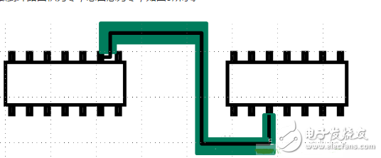
The current must flow in one loop. Each signal has a reflow to form a loop. At DC and low frequencies, the loop current always passes through the path with the least resistance; at high frequencies, the reflow always passes through the path with the least impedance.
The two wires respectively flow through the signal currents of opposite magnitude and opposite direction, and their magnetic fields are also equal in magnitude. If the distance between the two wires is very close, the magnetic field, ie differential mode EMI radiation, will completely cancel out. So the basic principle is: if the differential mode EMI radiation is to be minimized, the signal line should be as close as possible to the return line that forms the loop, ie the loop area must be minimized.
Careful routing design can greatly reduce the disturbance caused by the trace impedance and suppress the electromagnetic disturbance emission. When the frequency exceeds a few kHz, the impedance of the wire is mainly determined by the inductance of the wire, and the thin and long loop wire exhibits high inductance (typically lOnH/cm), and its impedance increases with frequency. If the design is not handled properly, it will cause co-impedance coupling.
Two parallel wires with opposite current directions can effectively reduce inductance due to mutual inductance. The total self-inductance can be expressed as:
L = L1 + L2 - 2M
Where L1 and L2 are the self-inductance of wire 1 and wire 2, respectively, and M is mutual inductance.
M=L1/[1+(a/h)2]
Where a-spacing, h-distance from the ground. When: L1 = L2, then:
L = 2 (L1- M)&nbsnbsp;
When: a = 0
M = L1
, then L = 0.
The basic principle of wiring can be obtained, that is, the loop area is zero. For example, the distance between the layers of the multi-layer board is very small, the 4-layer board is 0.15 mm, and the 28-layer board is 0.05 mm. The loop area is truly zero, and the total self-inductance is zero, as shown in FIG.
Figure 3 Basic principle of wiring: zero loop area
In the layout of the printed board, physical partitioning and electrical partitioning should be performed first to determine the position of the components on the board, then the grounding and power lines are arranged, then the high-speed signal lines are arranged, and finally the low-speed signal lines are considered.
In the layout, first make the incompatible segmentation, the position of the components should be grouped according to the power supply voltage, digital and analog circuits, speed, current, etc., so as to avoid mutual harassment. The arrangement of the individual pins of the printed board connector can be determined based on the location of the components. All connectors should be placed on one side of the printed board, avoiding cables from both sides and reducing common mode emissions. Secondly, the requirements should be met in terms of installation, stress, heat and aesthetics.
(1) Power cord
In consideration of safety conditions, the power line should be as close as possible to the ground line to reduce the ring area of ​​the differential mode radiation, and also help to reduce the crosstalk of the circuit. For a single power supply PCB, one power plane is sufficient; for multiple power supplies, if they are not interlaced, consider splitting the power plane. When used as a reference plane, add a capacitor. For power supply interleaving (especially multiple power supplies) For boards with power supply and interleaved ICs, two or more power planes must be considered.
(2) Location of clock line, signal line and ground line
The clock line and the signal line are adjacent to the ground plane or close to the ground line, and the loop area formed is as small as possible. If necessary, escort the ground on both sides.
(3) Split by logical speed
When fast, medium, and low-speed logic circuits need to be placed on a board, high-speed devices (fast logic, clock oscillators, etc.) should be placed close to the edge connector, while low-speed logic and memory should be placed away from Within the connector range. This is advantageous for the reduction of common impedance coupling, radiation and crosstalk.
(4) Avoid the discontinuity of the characteristic impedance of the printed circuit board, and ensure that the characteristic impedance is continuous. The trace width should not be abrupt, the wire should not be suddenly cornered, the width of the same layer of wiring must be continuous, and the trace impedance of different layers. Must also be continuous.
(5) Check whether the length of the signal line and the frequency of the signal constitute resonance, that is, when the wiring length is an integral multiple of the signal wavelength 1/4, the wiring will resonate, and the resonance will radiate electromagnetic waves, causing disturbance.
2. High-speed digital circuit design
In electronic systems, traces of various lengths are required. On these traces, it takes time for the signal to travel from the beginning of the line to the terminal. In other words, there is a delay in the signal. This delay can be ignored in low speed systems; however, in high speed systems it cannot be ignored. High-speed PCB design also needs to consider when the signal is transmitted on the wire. If the transmission line does not match the impedance of the start end or the terminal impedance, electromagnetic wave reflection will occur, the signal will be distorted, and the interference pulse will be generated, which will affect the system operation.
The so-called high-speed PCB is from the perspective of digital circuits, and for analog circuit PCBs, it is a high-frequency problem. High speed refers to the high edge rate of the signal, not necessarily the high clock frequency. It can be said that a PCB with a low clock frequency is not necessarily a high-speed PCB, and a PCB with a high clock frequency must also be a high-speed PCB. Once the designed PCB is designed as a high-speed PCB, it is necessary to consider the issues of high-speed signal transmission, termination, crosstalk, etc. If this is not the case, without the high-speed signal integrity design, the PCB's operational reliability may be There is no guarantee or even work. For ordinary PCBs, it doesn't matter if you don't consider the impact of high speed.
Signal Integrity (SI) refers to the accuracy of signal quality and signal timing on the signal line. That is, within the required time, the signal can respond with the required timing, duration, and voltage amplitude, and the signal is complete without distortion from the source to the receiver. Therefore, signal integrity analysis is based on voltage waveform analysis.
Timing is a core issue in high-speed systems. If the timing is not accurate, you cannot get accurate logic. Any delay or waveform distortion that occurs at the driver, interconnect or receiver when the signal is transmitted can cause the transmission to fail.
The reasons for the destruction of signal integrity are: the switching speed of the chip used is too fast; the arrangement of the termination components is unreasonable, the circuit interconnection is unreasonable, and the impedance caused by the transmission line, via hole, etc. is discontinuous; the crosstalk caused by the line spacing is too small and the peak Voltages, etc. can cause signal integrity problems. Signal integrity issues include reflection, crosstalk, overshoot, oscillation, delay, and electromagnetic disturbance emissions. The goal of signal integrity analysis is to ensure reliable high-speed data transmission. The key to the success of high-speed digital system design is to maintain signal integrity. Broadly speaking, signal integrity issues refer to all the problems caused by interconnects in high-speed products. It focuses on how interconnect performance affects product performance when interacting with digital signal voltage and current waveforms. Signal integrity issues include:
Reflected signal
Delay & Timing errors Delay & TIming errors
Overshoot/Undershoot
Ringing (multiple crossing logic level threshold error False switching)
Crosstalk Induced Noise (or crosstalk)
Electromagnetic radiation EMI radiaTIon
In order to achieve signal integrity, S must be shortened and impedance matching is performed. The impedance matching methods are: series resistance, parallel resistance, Thevenin network, RC network, diode array, etc.
Second layer grounding design
one. Grounding design is an important layer of importance.
1. Grounding refers to the connection of a circuit, device, sub-system to a reference ground in order to provide an equipotential point or surface. Grounding must be done with a grounding conductor and ground reference.
2. The meaning of the reference ground is extensive, it can be the earth, or it can be a conductor with a sufficient area to function as a ground. Such as the shell of an aircraft or ship, the cabinet of a cabinet, etc. The ideal reference ground is a zero-potential, zero-impedance physical body. It can provide a reference potential for a circuit or system; it can suppress electromagnetic disturbances generated inside the product and external electromagnetic interference into the product; and can provide a low impedance path for the current to flow back to the source.
3 Grounding is a system concept. Current amplitude and frequency are two key factors. The grounding classification is to select the grounding body and its connection method.
Grounding classification grounding current amplitude grounding current frequency range
Signal ground (return ground) several mA - several A DC - GHz
Power supply a few mA - a few A "50-60Hz
Protected ground (safely) 10A-1000A "50-60Hz
Lightning protection "240kA 200kHz-500MHz
Reference ground (EMI ground) μA-A DC-microwave
One of the reference tasks is to provide a controlled suppression channel for EMI currents. The key is to maintain low impedance over a very wide frequency range.
Lightning protection provides a controlled channel that directs lightning currents into the ground. The key is to maintain low resistance and low inductance at the same time, and to provide sufficient transient current capacity.
Safely (protected ground) is mainly to protect personal safety. The metal housing is usually grounded to ensure that fault currents flow into the ground in the event of a fault.
The main problem with the power ground is to maintain low impedance and provide sufficient current capacity.
Signal ground (return ground) provides a return path for the signal
two. Grounding method
Suspended ground
When the signal level is large or close, the module should be connected to the system ground. When the signal level is small or the phase difference is large, the low-level signal module should be connected to the floating ground.
The ground wire of the equipment suspension equipment is electrically insulated from the reference ground and other conductors.
Unit circuit floating ground unit circuit signal ground is insulated from reference ground and chassis
Suspension is prone to static buildup and electrostatic discharge. Easy to be struck by lightning and other transient disturbances. A large resistance is usually connected between the floating ground and the reference ground to eliminate static electricity accumulation.
2. Single point grounding (f "1MHz")
Parallel single-point grounding: Each circuit module is connected to a single point ground, and each unit is connected to the reference point at the same point.
Series single-point grounding of multi-stage circuits: The grounding point should be selected at the input of the low-level circuit to be closest to the reference ground. If the ground point is moved to the high level, the potential difference between the ground of the input stage and the reference ground is the largest and unstable.
3. Multi-point grounding (f 》10MHz)
The circuits in the device are all close to the chassis, and all the chassis are ground referenced to minimize the length of the ground lead. In the case of multi-point grounding, pay attention to the ground loop problem. When the signal frequency is between 1-10MHz and the local line length does not exceed l / 20, a single point grounding can be used, otherwise multiple points should be grounded. The length of the local line can be compared with l/4, which becomes the l/4 transmission line of the terminal short circuit, equivalent to an open circuit, and the impedance increases.
4. Hybrid grounding
The use of reactive components allows the grounding system to exhibit different characteristics at low and high frequencies.
The hybrid grounding of electronic equipment divides the ground of the equipment into two categories: power ground and signal ground. Each part of the power ground of the equipment is connected to the total ground of the power supply and the total ground of the signal is collected to the common reference ground.
three. Long ground impedance
1. Ground impedance is the root cause of ground harassment
The ideal ground should be a zero-potential, zero-impedance physical entity. However, the actual ground wire itself has both a resistive component and a reactance component. When a current flows through the ground wire, a voltage drop is generated. The ground line forms a loop with other connections (signals, power lines, etc.). When the electromagnetic field is coupled to the circuit, an induced electromotive force is generated in the ground loop and coupled to the load by the ground loop, posing a potential EMI threat.
Transmission line input impedance
Zin(x)=Zc(ZL+jZctgβx)/(Zc+jZLtgβx)
Where β = 2π / λ = ω (LC) 1/2,
When ZL=0
∣Zin(x)∣=∣jZctgβx∣=Zctg(ωx(LC)1/2)
When x=λ/4
∣Zin(x)∣=Zctg[ω(λ/4)(LC)1/2]=Zctg(π/2)=∞
At this time, the ground line is actually open, but instead becomes an antenna that radiates outward.
2 ground length
The length of the ground wire should be: ≤ l / 20 should be short and thick.
Third layer structure / shielding design

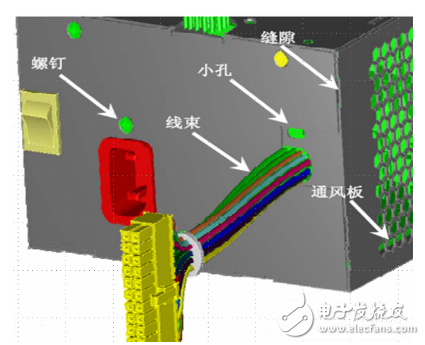
The electromagnetic compatibility design of the product should be both at the same time. The interface between the product and the outside world is shown in Figure 4. Including chassis port, power line port, ground port, signal line port and control line port. Structural/shield design, filter design, and transient disturbance suppression design are required.
Figure 4 interface between the product and the outside world
What is structure? Structure is the sum of materials, shapes, connections, and layouts.
For a single part, the structure is the material and shape of the part. The material contains the intrinsic structure of the part; the shape reflects the extrinsic features of the part.
For two or more parts, the connection between them is also included, and the "connection" is the method of assembly between the parts.
For the whole machine, we must also consider the layout of the components.
The structure design is expressed and calculated by engineering drawings or parameterized electronic documents, submitted to the manufacturing, and the product is produced. Including the machine shape, layout, component connections, materials and standard parts and general parts selection.
The difference between an electronic product structure and a purely mechanical structure is that the electromagnetic compatibility of the structure is also considered.
Shielding technology is used to suppress the propagation of electromagnetic disturbances above 10 kHz along the space, that is, to cut off the coupling path of radiative disturbance.
one. Shielding effectiveness concept
Shields for electromagnetic compatibility purposes typically attenuate the intensity of electromagnetic disturbances to one-hundredth to one-millionth of the original. For convenience, the performance of the shield is expressed in terms of shielding effectiveness SE or SH (dB). Defined as: SE=20lg(E1/E2)(dB)
SH=20lg(H1/H2)(dB)
In the formula, E1 and H1 are respectively the electric field strength and the magnetic field strength measured when unshielded, and E2 and H2 are respectively the electric field strength and the magnetic field strength measured after shielding.
The overall shielding effectiveness of the shield is determined by the weakest link in the shield. In order to achieve a certain value of the shielding effectiveness of the shielding body, all parts of the shielding body must reach this value, that is, the matching of the shielding effectiveness of each part is very important.
The weakest link in the shield is the various gaps and holes.
To achieve shielding, first of all, the first and second layers of the "electromagnetic compatibility layering and comprehensive design method" should be done to minimize the electromagnetic emission and maximize the anti-interference ability. The housing is then used to cut off EMI radiation.
However, with this definition, only the shielding effectiveness of the shield can be tested, and it is not possible to determine what material should be used to make the shield. To determine what material should be used to make the shield, you need to know what the shielding effectiveness of the material is related to what the material is.
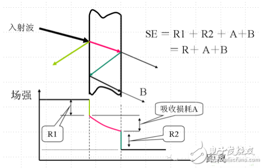
1 Calculation of shielding effectiveness of solid materials
The solid shield sees the shield as an infinitely large or fully enclosed housing that is structurally complete and electrically continuous, with no electrical discontinuities such as holes or gaps. The solid shielding theory reflects the "ideal shielding effectiveness" that the shielding material can achieve under "solid" conditions, and only guides the development and selection of shielding materials. The calculation of the shielding effectiveness of solid materials is shown in Figure 5.
When electromagnetic waves are incident on an infinite flat shield, part of the energy is reflected, called reflection loss, which is denoted as R1; the transmitted wave is attenuated when propagating in the metal plate, and is called absorption loss, which is recorded as A. The electromagnetic wave reaches the shield and another On the side, it is again recorded as R2, and only a small amount of energy is transmitted into the shielded space. The reflected energy is again attenuated and reflected, cycling back and forth until the energy is all attenuated and transmitted. This phenomenon of multiple reflection, called the multiple reflection correction coefficient, is recorded as B, and the magnitude is less than 1.
The grounding shield made of good conductors such as silver, copper, aluminum, nickel, etc. can shield the electric field and the high-frequency magnetic field; when the thickness is small and the frequency is low, the shielding effectiveness of the steel is lower than that of copper; when the thickness is large and the frequency is high The shielding effectiveness of steel is higher than that of copper; when the thickness is above 0.67mm, the shielding effectiveness of steel is higher than that of copper. For near-field electric field shielding, copper is preferred.
For f "100kHz low frequency magnetic field, it is shielded with high magnetic permeability material, such as industrial pure iron, iron silicon alloy (silicon steel, electrical steel, etc.), iron nickel soft magnetic alloy, permalloy (79c / o nickel, 21c / o iron ), amorphous soft magnetic alloy material (having high strength, high hardness, high ductility, corrosion resistance), μ metal, ferrite material, etc.
Figure 5 Calculation of shielding effectiveness of solid materials
2 The level of the shielding scheme: the lower the level, the easier it is to achieve high shielding effectiveness.
Single board shielding and partial shielding of the board: about 20dB/1GHz
Module shielding: Modules with large radiation disturbance or poor anti-harassing capability are installed separately in the shielding box. It is not only easy to implement, but also low in cost, and can reduce mutual harassment between modules and achieve electromagnetic compatibility between internal modules of products. About 20dB/1GHz
Plug-in, sub-rack shielding: about 20dB/1GHz
Cabinet shielding: about 15dB/1GHz
Figure 6 shows the shielding effectiveness of the assembled cabinet, 30-230MHz: 20dB; 230-1000MHz: 10dB
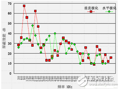
Figure 6 Shielding effectiveness of the assembled cabinet
two. Actual shield problem
There are many sources of electromagnetic leakage on the actual shielding body, for example, gaps at different joints, vents, display windows, buttons, indicator lights, cable lines, power lines, etc., as shown in Figure 7.
Figure 7 Electromagnetic leakage source on the actual shield
1 slit shielding
: When the length of the gap is close to half the wavelength, the electromagnetic wave will leak out. This type of electromagnetic leakage source is a slot antenna. When the gap size is close to an integral multiple of half a wavelength, the electromagnetic leakage is the largest. Therefore, special shielding should be done at high frequency, and the length of the slit or the hole diameter should be less than l/100. Electrical continuity must be maintained throughout the joint to avoid the formation of a slit antenna. At least every l/6 of the electrical contact between the mating surfaces - the direct connection of the fastening points (including screws, rivet spot welding, locks, etc.). Permanent seams using a welding process. The seam formed by the non-permanent mating surface is made of a conductive gasket. Both can reach 20dB/1GHz.
The conductive continuity of the shield is the most important factor affecting the shielding effectiveness.
2 ventilation hole treatment
The goal is to deal with the contradiction between shielding and heat dissipation.
The waveguide is a tubular metal structure with high-pass filter characteristics. High-frequency electromagnetic waves can pass through the waveguide, and electromagnetic waves with low frequency are greatly depleted. The waveguide operating in the cut-off zone is called a cut-off waveguide, and the disturbance frequency can be suppressed by falling within the cut-off zone. This type of device is called a cut-off waveguide louver, as shown in Figure 8, for cabinets that require high shielding effectiveness.
Figure 8 Cut-off waveguide ventilation window
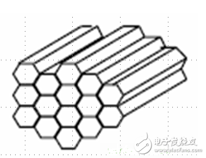
The cut-off waveguide vent window can suppress disturbances below 10 GHz, and the screen effect is 50-80 dB/1 GHz. However, the cost is high, and the aluminum waveguide is pasted and adhered to conductive treatment such as conductive oxidation, tin plating, nickel plating, etc., and the price is 1000 yuan. /m2 or more. Steel waveguides are made by brazing and are expensive and not recommended.
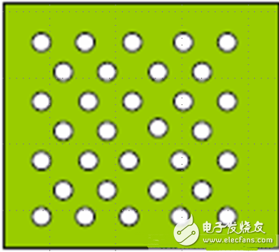
For cabinets with low shielding performance requirements, metal orifice plates can be used, as shown in Figure 9. Only applicable when the disturbance frequency is lower than 50MHz, the screen effect is 30-50dB/1GHz. The material is steel or aluminum.
Figure 9 metal orifice plate
3 display: metal coated conductive glass
The metal coated glass is formed by forming a dense conductive film on the surface of ordinary or tempered glass by vacuum sputtering or the like, and has the advantages of high shielding efficiency, high light transmittance, no optical distortion, and strong environmental adaptability.
4 cable or wire through the shield
The filter connector is used for multiple wires or cables to traverse the shield. The feedthrough capacitor and feedthrough filter are used to traverse the shield with a single wire or cable.
5 continuous design
The correct connection of the shielding layer should be crimped and 360 degree overlap to form a dumbbell-shaped structure, which becomes an extension of the shielding case.
Fourth layer filter design
Conducted disturbances can be transmitted through conductors such as power lines, signal lines, and interconnects, as well as conductors such as shields and grounding conductors. The solution to conductive coupling is to remove the disturbance from the wire or conductor by filtering before the disturbance enters the sensitive circuit.
Electromagnetic disturbance filters, or EMI filters, are the most effective means of suppressing conducted disturbances. It includes a signal line filter and a power line filter. The signal line filter allows the useful signal to pass without attenuation while greatly attenuating the clutter disturbance signal. The power line filter, also known as the power grid filter, transmits DC, 50 Hz, and 400 Hz power to the device with a small attenuation, but greatly attenuates the EMI signal transmitted through the power supply to protect the device from damage. At the same time, it can suppress the EMI signal generated by the device itself, prevent it from entering the power grid, pollute the electromagnetic environment, and harm other devices.
An EMI filter, usually a lumped-parameter, passive low-pass filter. However, the EMI filter is different from the general low-pass filter, and the EMI filter is more concerned with the characteristics of insertion loss, energy attenuation, and cutoff frequency.
A key feature that affects filter performance
1.å½±å“滤波器性能的关键特性之一:阻抗特性
æ— æºæ»¤æ³¢å™¨ç”±æŠ‘制元件组æˆï¼Œå…¶æŠ‘制特性ä¸ä»…å–决于元件å‚数,而且还å–决于端接阻抗。 如图10所示。
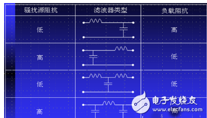
图10 æº/负载阻抗与滤波器网络结构的选择
例如,为防æ¢ç”µæºç³»ç»Ÿçš„ä¸ç¨³å®šæ€§ï¼Œæ»¤æ³¢å™¨çš„输出阻抗必须å°äºŽå¼€å…³ç”µæºå¼€çŽ¯è¾“入阻抗。滤波器的输入阻抗应与电网输出阻抗相差较大。其目的是为了尽å¯èƒ½ä½¿ä¹‹å¤±é…,以获得尽å¯èƒ½å¤§çš„æ’å…¥æŸè€—。
2.å½±å“滤波器性能的关键特性之二:频率特性
EMIæ»¤æ³¢å™¨çš„æŠ‘åˆ¶å™ªå£°èƒ½åŠ›çš„è¯„å®šæŒ‡æ ‡ï¼šæ’å…¥æŸè€—IL(Insertion Loss)。æ’å…¥æŸè€—的定义如图11所示。
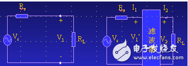
图11 æ’å…¥æŸè€—的定义
共模和差模æ’å…¥æŸè€—是在50~75Wé—´çš„æŸä¸€é˜»å€¼çš„系统内进行测é‡çš„,是最优化和误导,100/0.1Ω或0.1/100Ω系统æ‰èƒ½çœŸå®žåœ°é¢„估实际应用时的性能。
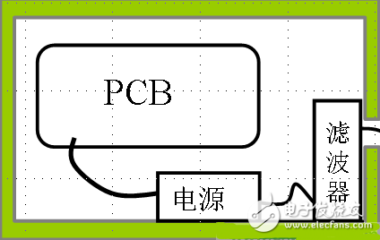
3.å½±å“滤波器性能的关键特性之三:电æºçº¿æ»¤æ³¢å™¨çš„安装
电æºçº¿æ»¤æ³¢å™¨å®‰è£…时,容易出现的问题包括,滤波器输入线过长ã€è¾“入输出å‘生耦åˆã€æŽ¥åœ°ä¸è‰¯ç‰ã€‚针对这些问题,电æºçº¿æ»¤æ³¢å™¨çš„æ£ç¡®å®‰è£…应当如图12所示。
图12 电æºçº¿æ»¤æ³¢å™¨çš„æ£ç¡®å®‰è£…
第五层瞬æ€éªšæ‰°æŠ‘制设计
一.电快速瞬å˜è„‰å†²ç¾¤ï¼ˆEFT)的抑制
抑制EFTå¿…é¡»åšåˆ°ï¼šæ£ç¡®é€‰ç”¨å’Œå®‰è£…电æºæ»¤æ³¢å™¨å’Œä¿¡å·æ»¤æ³¢å™¨ï¼šå‡å°PCB环路é¢ç§¯å’Œå¼•çº¿ç”µæ„Ÿ;分类æ†æ‰Žåˆ†ç±»æ•·è®¾å¯¼çº¿å’Œç”µç¼†;控制线使用å±è”½çº¿ï¼Œç”µæºçº¿ä¸åº”过长;æ£ç¡®åšå¥½æŽ¥åœ°è®¾è®¡ï¼›å®‰è£…瞬æ€éªšæ‰°æŠ‘制器。
二.雷击浪涌的抑制
导致雷击浪涌试验失败表现在过高的差模电压导致输入器件被击穿,或过高的共模电压导致线路与地之间的ç»ç¼˜å±‚被击穿。
通过雷击浪涌æ•æ„Ÿåº¦è¯•éªŒåº”采å–的措施:浪涌å¸æ”¶å™¨ä»¶è¦ç”¨åœ¨è¿›çº¿å…¥å£å¤„。在器件附近ä¸èƒ½æœ‰ä¿¡å·çº¿å’Œç”µæºçº¿ç»è¿‡ï¼Œä»¥é˜²æ¢å°†æµªæ¶Œå¼•å…¥ä¿¡å·å’Œç”µæºçº¿è·¯ã€‚器件的引脚è¦çŸï¼›å¸æ”¶å®¹é‡è¦ä¸Žæµªæ¶Œç”µåŽ‹å’Œç”µæµçš„试验ç‰çº§ç›¸åŒ¹é…。
三。é™ç”µé˜²æŠ¤
é™ç”µæ”¾ç”µæ˜¯é«˜ç”µä½ã€å¼ºç”µåœºã€çž¬æ€å¤§ç”µæµçš„过程。所产生的上å‡æ—¶é—´æžå¿«ã€æŒç»æ—¶é—´æžçŸï¼ˆå¤šæ•°åªæœ‰å‡ 百纳秒)的电ç£è„‰å†²ã€‚
1. ESD防护是一项系统工程,需è¦å„个环节实施全é¢æŽ§åˆ¶ã€‚一般应达到(+/-)2000V以上的防护è¦æ±‚。
2.电å设备ESDä¿æŠ¤ç”µè·¯è®¾è®¡
æ—路释放ä¿æŠ¤ç”µè·¯ï¼šå…¶ä½œç”¨æ˜¯å°†é™ç”µè·é€šè¿‡è¯¥ä¿æŠ¤ç”µè·¯é‡Šæ”¾æŽ‰ï¼Œé¿å…对功能元器件的é™ç”µæŸä¼¤ï¼›é™åŽ‹/é™æµä¿æŠ¤ç”µè·¯ï¼šå…¶ä½œç”¨æ˜¯å‡ç¼“é™ç”µçš„放电速度,使放电电压/æµå°ä¸€äº›ï¼Œé’³åˆ¶å™¨ä»¶ç«¯å£çš„电ä½ï¼›é‡‡ç”¨ç»ç¼˜ä»‹è´¨å¦‚塑料机箱ã€ç©ºæ°”é—´éš™åŠç»ç¼˜ææ–™ç‰æŠŠå†…部系统和元器件与外界隔离;。使用金属å±è”½å¤–壳,防æ¢å¤§çš„ESD电æµå†²å‡»å†…部电路;.PCBæ¿ä¸Šå®‰è£…光耦åˆå™¨ã€éš”离å˜åŽ‹å™¨ã€å…‰çº¤/æ— çº¿å’Œçº¢å¤–çº¿è€¦åˆï¼Œå®žçŽ°ç”µæ°”隔离。
四.瞬æ€éªšæ‰°æŠ‘制器
由于滤波器的输入输出阻抗与电网以åŠè´Ÿè½½é˜»æŠ—严é‡å¤±é…,对瞬æ€éªšæ‰°çš„抑制能力éžå¸¸æœ‰é™ã€‚ç›®å‰æœ€æœ‰æ•ˆçš„办法是采用瞬æ€éªšæ‰°æŠ‘制器,将大部分能é‡è½¬ç§»åˆ°åœ°ã€‚
1.é¿é›·ç®¡ï¼šæ—©æœŸçš„é¿é›·ç®¡æ˜¯æ°”体放电管,一个电æžæŽ¥å¯èƒ½è€¦åˆçž¬æ€éªšæ‰°çš„线路,å¦ä¸€ä¸ªæŽ¥åœ°ã€‚瞬æ€éªšæ‰°å‡ºçŽ°æ—¶ï¼Œç®¡å†…气体被电离,两æžé—´çš„电压迅速é™åˆ°å¾ˆä½Žçš„残压值(2-4kV)上,使大部份瞬æ€èƒ½é‡è¢«åœ°çº¿è¿…速转移,通æµå®¹é‡å¤§ï¼ˆ100kA以上),功耗大大é™ä½Žï¼Œæ¼ç”µæµå°ï¼Œäº§å“å—到了ä¿æŠ¤ã€‚ç›®å‰å·²å›ºåŒ–,体积很å°ã€‚é¿é›·ç®¡å…·æœ‰å¾ˆå¼ºçš„浪涌电æµå¸æ”¶èƒ½åŠ›ï¼Œå¾ˆé«˜çš„ç»ç¼˜ç”µé˜»ï¼ˆã€‹104MW)和很å°çš„寄生电容(《2pF),对产å“æ£å¸¸å·¥ä½œä¸ä¼šäº§ç”Ÿæœ‰å®³å½±å“。但其å“应时间较慢,约为£100ns.åªé€‚用于线路ä¿æŠ¤å’Œäº§å“的一次ä¿æŠ¤ã€‚
2.压æ•ç”µé˜»å™¨ï¼ˆVSR)(varistor; voltage-dependent resistor):为多个PN结并è”和串è”在一起的电压æ•æ„Ÿåž‹ç®ä½ä¿æŠ¤å™¨ä»¶ã€‚å½“åŠ åœ¨å…¶ä¸¤ç«¯çš„ç”µåŽ‹ä½ŽäºŽæ ‡ç§°åŽ‹æ•ç”µåŽ‹æ—¶ï¼Œå…¶ç”µé˜»è¿‘ä¸ºæ— ç©·å¤§ï¼Œè€Œè¶…è¿‡æ ‡ç§°åŽ‹æ•ç”µåŽ‹å€¼åŽï¼Œé˜»å€¼ä¾¿æ€¥å‰§ä¸‹é™ã€‚它对瞬æ€ç”µåŽ‹çš„å¸æ”¶ä½œç”¨æ˜¯é€šè¿‡ç®ä½æ–¹å¼å®žçŽ°çš„,并转æ¢ä¸ºçƒé‡ã€‚å…¶å“应时间《50ns.主è¦å‚数为:
1)ã€æ ‡ç§°åŽ‹æ•ç”µåŽ‹V1mA ,å³å‡»ç©¿ç”µåŽ‹æˆ–阈值电压。指在1mA规定电æµä¸‹çš„电压值,å³1mAç›´æµæ—¶æµ‹å¾—的电压值。为10ï¼9000Vä¸ç‰ã€‚一般V1mA=1.5Vp或V1mA=2.2VAC,å¼ä¸ï¼ŒVp为电路é¢å®šç”µåŽ‹çš„峰值。VAC为é¢å®šäº¤æµç”µåŽ‹çš„有效值。ZnO压æ•ç”µé˜»çš„电压值选择是至关é‡è¦çš„,它关系到ä¿æŠ¤æ•ˆæžœä¸Žä½¿ç”¨å¯¿å‘½ã€‚如é¢å®šç”µæºç”µåŽ‹ä¸º220V,则压æ•ç”µåŽ‹V1mA=1.5Vp=1.5×1.414×220V=467V,或V1mA=2.2VAC=2.2×220V=484V.å› æ¤ï¼Œé€‰åœ¨470ï¼480V之间。
2)ã€é€šæµå®¹é‡ï¼ˆkA) ,å³åœ¨çŽ¯å¢ƒæ¸©åº¦ä¸º25℃情况下最大脉冲电æµçš„峰值,通常选用2ï¼20kA。
3)〠残压比:规定峰值为8/20msæ ‡å‡†å†²å‡»ç”µæµé€šè¿‡åŽ‹æ•ç”µé˜»åŽï¼Œ 两端的峰值电压值(称为最大é™åˆ¶ç”µåŽ‹ï¼‰ä¸ŽåŽ‹æ•ç”µåŽ‹ä¹‹æ¯”。约为1.7-1.8.
3.TVS(Transient Voltage Suppresser瞬æ€ç”µåŽ‹æŠ‘制器)
éšç€ç”µåä¿¡æ¯æŠ€æœ¯çš„迅速å‘展,当å‰åŠå¯¼ä½“器件日益趋å‘å°åž‹åŒ–ã€é«˜å¯†åº¦å’Œå¤šåŠŸèƒ½åŒ–ã€‚å› æ¤è¦æ±‚ä¿æŠ¤å™¨ä»¶å¿…须具备低ç®ä½ç”µåŽ‹ä»¥æ供有效的ESDä¿æŠ¤ï¼›è€Œä¸”å“应时间è¦å¿«ä»¥æ»¡è¶³é«˜é€Ÿæ•°æ®çº¿è·¯çš„è¦æ±‚ï¼›å°è£…集æˆåº¦é«˜ä»¥é€‚用便æºè®¾å¤‡å°åˆ¶ç”µè·¯æ¿é¢ç´§å¼ 的情况;åŒæ—¶è¿˜è¦ä¿è¯å¤šæ¬¡ESD过程åŽä¸ä¼šåŠ£åŒ–以ä¿è¯é«˜æ¡£è®¾å¤‡åº”有的å“质。TVS(Transient Voltage Suppresser瞬æ€ç”µåŽ‹æŠ‘制器)æ£æ˜¯ä¸ºè§£å†³è¿™äº›é—®é¢˜è€Œäº§ç”Ÿçš„,它已æˆä¸ºä¿æŠ¤ç”µåä¿¡æ¯è®¾å¤‡çš„关键性技术器件,是专门设计用于å¸æ”¶ESD能é‡å¹¶ä¸”ä¿æŠ¤ç³»ç»Ÿå…éESDæŸå®³çš„固æ€å…ƒä»¶ã€‚
TVS是一ç§äºŒæžç®¡å½¢å¼çš„高效能ä¿æŠ¤å™¨ä»¶ã€‚当TVS二æžç®¡çš„两æžå—到åå‘瞬æ€é«˜èƒ½é‡å†²å‡»æ—¶ï¼Œå®ƒèƒ½ä»¥10-12秒é‡çº§çš„速度,将其两æžé—´çš„高阻抗å˜ä¸ºä½Žé˜»æŠ—,å¸æ”¶é«˜è¾¾æ•°åƒç“¦çš„浪涌功率,使两æžé—´çš„电压ç®ä½äºŽä¸€ä¸ªé¢„定值,有效地ä¿æŠ¤ç”µå线路ä¸çš„精密元器件,å…å—å„ç§æµªæ¶Œè„‰å†²çš„æŸå。由于它具有å“应时间快ã€çž¬æ€åŠŸçŽ‡å¤§ã€æ¼ç”µæµä½Žã€å‡»ç©¿ç”µåŽ‹åå·®å°ã€ç®ä½ç”µåŽ‹è¾ƒæ˜“控制ã€æ— æŸåæžé™ã€ä½“积å°ç‰ä¼˜ç‚¹ã€‚
ç›®å‰å·²å¹¿æ³›åº”用于计算机系统ã€é€šè®¯è®¾å¤‡ã€äº¤/ç›´æµç”µæºã€æ±½è½¦ã€ç”µå镇æµå™¨ã€å®¶ç”¨ç”µå™¨ã€ä»ªå™¨ä»ªè¡¨ï¼ˆç”µåº¦è¡¨ï¼‰ã€RS232/422/423/485ã€I/Oã€LANã€ISDNã€ADSLã€USBã€MP3ã€PDASã€GPSã€CDMAã€GSMã€æ•°å—照相机的ä¿æŠ¤ã€å…±æ¨¡/差模ä¿æŠ¤ã€RF耦åˆ/IC驱动接收ä¿æŠ¤ã€ç”µæœºç”µç£éªšæ‰°æŠ‘制ã€å£°é¢‘/视频输入ã€ä¼ 感器/å˜é€Ÿå™¨ã€å·¥æŽ§å›žè·¯ã€ç»§ç”µå™¨ã€æŽ¥è§¦å™¨å™ªéŸ³çš„抑制ç‰å„个领域。
第å…层系统级电ç£å…¼å®¹è®¾è®¡
EMC对系统效能的影å“包括:系统性能é™ä½Žæˆ–失效;系统å¯é 性é™ä½Žï¼›å½±å“系统工作寿命;影å“效/费比的æƒè¡¡ï¼›å½±å“系统和人员的生å˜æ€§å’Œå®‰å…¨æ€§ï¼›å»¶è¯¯ç”Ÿäº§å’Œä½¿ç”¨ã€‚系统级电ç£å…¼å®¹è®¾è®¡æµç¨‹å¦‚图13所示。
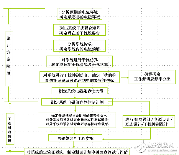
图13 系统级电ç£å…¼å®¹è®¾è®¡æµç¨‹
实践表明,满足了设备EMCé™å€¼çš„设备ã€åˆ†ç³»ç»Ÿç»„æˆç³»ç»ŸåŽå¹¶ä¸èƒ½ä¿è¯ç³»ç»Ÿçš„EMC良好,å³EMC+EMC¹EMCã€‚å› æ¤è§„定系统的EMCè¦æ±‚并实现它是与ä¿è¯è®¾å¤‡EMCåŒç‰é‡è¦çš„。例如,如果N个模å—分别在场点测得的场强值基本相ç‰ï¼Œåˆ™
Eo=N1/2E(mV/m)
è®¾æ ‡å‡†è§„å®šçš„éªšæ‰°å‘å°„é™å€¼ä¸ºEo,若有N个模å—,则æ¯ä¸ªæ¨¡å—的骚扰å‘å°„é™å€¼åº”为
E=Eo/N1/2
å余年æ¥ï¼Œâ€œç”µç£å…¼å®¹åˆ†å±‚与综åˆè®¾è®¡æ³•â€å·²æˆåŠŸç”¨äºŽï¼Œåˆæˆå”径雷达å«æ˜Ÿã€å¤§åž‹é›†è£…箱检查系统ã€æ‰‹æŒæœºã€é›†æˆç”µè·¯ã€æ±½è½¦ç”µå系统ã€åŒ»ç”¨ç”µå设备与系统ã€åµŒå…¥å¼æœºå™¨äººæŽ§åˆ¶å™¨ç‰çš„电ç£å…¼å®¹è®¾è®¡ï¼ŒåŸºæœ¬åšåˆ°ç”µç£å…¼å®¹è¯•éªŒä¸€æ¬¡æˆåŠŸã€‚
Perfect fit: The Hydrogel Screen Protector is designed with a Soft TPU material, which can be completely covered even on a curved device, providing perfect protection for the full coverage of the screen.
Oleophobic and waterproof: The use of hydrophobic and oleophobic screen coatings can prevent sweat, grease residue and fingerprints without reducing screen sensitivity. It is almost invisible on the screen and brings a high-definition visual experience.
Sensitive touch: ultra-thin and Soft Hydrogel Film with a thickness of only 0.14mm. As time goes by, it will self-repair minor scratches, provide you with a highly responsive screen protector and maintain the original touch.
Easy to install: The installation of the Protective Film is very simple, without air bubbles. The protective sticker can stay on the phone perfectly, and the bubbles will disappear within 24 hours.
If you want to know more about Hydrogel Screen Protector products, please click the product details to view the parameters, models, pictures, prices and other information about Hydrogel Screen Protective Film.
Whether you are a group or an individual, we will try our best to provide you with accurate and comprehensive information about the Hydrogel Protective Film!
Hydrogel TPU Protective Film,Ultra-Thin Protective Film,Soft Hydrogel Film,Hydrogel Film Screen Protector,Screen Protective Film,Mobile Phone Screen Guards
Shenzhen Jianjiantong Technology Co., Ltd. , https://www.jjtscreenprotector.com