The audio exchange hybrid matrix is ​​the core equipment of various conference, broadcast and command systems. It connects different audio input and output devices, realizes audio exchange and mixing functions, and realizes audio signal control and scheduling.
The traditional audio matrix is ​​usually based on the analog switch circuit design, the design is complex, and the implementation is difficult, and it is not suitable for constructing medium and large-scale switching matrices. Moreover, most matrices do not have volume adjustment and signal mixing functions, and need to be used with mixers and signal mixer devices.
This article refers to the address: http://
This paper proposes a design scheme of audio exchange hybrid matrix based on FPGA (Field ProgrammableGate Array). Based on the principle of switching technology, the scheme uses digital audio signal sampling and processing technology to construct a switching hybrid matrix, which realizes the exchange and mixing of 16 × 16 channels of audio signals. It is difficult to design and implement, and can be reduced or increased according to system requirements. System switching capacity, setting audio signal sampling accuracy and sampling rate; the volume of each input and output signal can be controlled independently; it also has low input and output delay, high isolation between channels and good sound quality.
1 Mathematical model of audio exchange mixing matrix
1. 1 Principle of the exchange system
Switching technology originates from telephone communication, and its basic task is to achieve end-to-end effective transmission of information between users in a large-scale network. The principle of the switching technology is to control the source data to be sent to the destination end by setting a good path.
For audio systems, switching refers to the forwarding of audio signals from the input through a series of nodes to the output.
1. 2 exchange mixed matrix mathematical model
Based on the principle of switching technology described in 2.1, a general mathematical model of the switching system can be constructed. The multi-input and output switching system is abstracted into a matrix P whose input and output signals are abstracted into two vectors (x, y). The function implemented by the switching system is to convert the input vector into a output vector through the operation of the matrix:
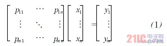
Where pij ∈[0, 1 ] represents the correspondence between input and output. n and m represent the number of input and output signals, respectively. When n = 1, the system is a single input system; when n > 1, the system is a multi-input system.
When m = 1, the system is a single output system; when m > 1, the system is a multi-output system.
For an audio exchange hybrid system, pij represents the correspondence between a certain input and a certain output, as well as the volume information. Finally, a separate output signal yj can be expressed as:

The core technology of this scheme is to convert multiple analog audio input signals into digital input vectors, and construct a digital exchange mixing matrix. The digital output vector is obtained by computing the matrix, and the output vector is converted into an analog audio output signal, and distributed to Each output port finally implements an audio exchange mixing matrix.
Here, let the vectors A and B be the input and output volume control vectors, respectively, and the matrix Q be the control matrix, then the switching matrix P is transformed into:
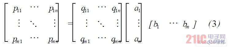
In summary, the final mathematical model for building the system is:
Where qji = 0, 1.
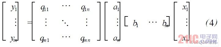
From equation (4), the final result yj of the jth output is:

2 System Design Overview
2. 1 system signal flow
According to formula (4) and formula (5), a system signal flow chart can be constructed, as shown in Fig. 1.
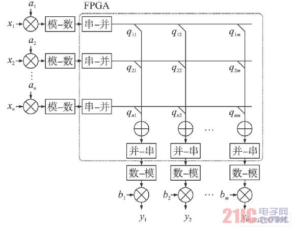
Figure 1 Signal flow diagram of a switched hybrid matrix system.
Ai and bj are implemented by a volume control chip, digital/analog and analog-to-digital conversion are implemented by dedicated chips, and matrix Q and multi-channel adders are implemented by FPGA.
The system switching capacity is set to 16 × 16, ie n = 16, m = 16. The switching capacity can be expanded or reduced for different system requirements.
2. 2 system hardware design
It can be known from the system signal flow diagram that the overall hardware module of the system is composed of input volume control, digital/analog conversion, exchange mixing matrix, analog/digital conversion, output volume control and the like. The overall hardware module block diagram of the system is shown in Figure 2.
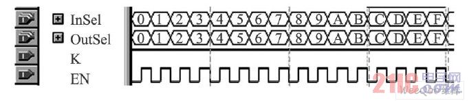
Figure 2 Block diagram of the overall hardware module of the exchange hybrid matrix.
The input volume control chip is PGA4311, and its gain adjustment range is 31. 5 dB~ - 95. 5 dB. It is controlled using the SPI bus.
The input analog/digital conversion chip uses PCM4204, which uses IO interface to control the working mode and parameters. See the literature for specific settings.
The output digital/analog conversion and volume control chip selects PCM1681, works in slave mode, and uses I2C interface to control it. See the literature for specific settings and methods of use.
By setting the analog/digital and digital/analog conversion chips, the sampling accuracy and frequency of the digital audio signal can be adjusted according to system requirements.
The sampling example of the solution in this paper has a sampling frequency of 97.7 kHz and a sampling accuracy of 24 bits. It is transmitted by left-aligned PCM coding. The transmission timing diagram is shown in Figure 3.

Figure 3 PCM code transfer timing (left justified).
2. 3 FPGA and its programming
The FPGA internally contains serial/parallel conversion, switching matrix, hybrid, parallel/serial conversion, clock module and matrix control module. The internal module block diagram is shown in Figure 4. The FPGA selects Altera's EP2C35 chip, and its specific parameters are listed in the literature.
2. 3. 1 clock module
The function of the clock module is to provide a unified global clock for the serial/parallel and parallel/serial conversion modules. There are three kinds of clock signals required by the system: system clock (SCK), bit clock (BCK) and channel clock (LRCK). Each clock frequency is determined by the sampling frequency (fS):
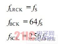

Figure 4 Block diagram of the internal FPGA block.
In this system, the sampling frequency fS is 97.7 kHz, and each of the above clocks is generated by dividing a 50 MHz external clock signal.
A 9-bit accumulation counter Q is built into the module to complete an up-count on the rising edge of the clock signal. When the value counts to the full value of 111111111, Q is set to 0 on the next clock cycle. Connect the XCLK, BCK, and LRCK outputs to bits 0, 2, and 8 of the count output, respectively, and combine bits 3 - 7 into another count output S_Count for controlling string-and-parallel-to-serial conversion Bit count. Therefore, the actual generated fSCK is 25 MHz, fBCK is 6.2 MHz, and fLRCK and fS are 97. 7 kHz.
2. 3. 2 Input String/Parallel Conversion Module
This module is responsible for converting the serial PCM code input by the PCM4204 into parallel data and feeding it to the switch fabric module for processing. The module is internally built through a 32-bit shift register (S_Buf) for storing serial data and controlling the parallel output based on the action of the channel clock (LRCK). The serial/parallel conversion process is shown in Figure 5.
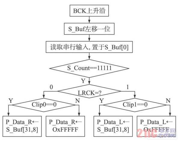
Figure 5 Serial/parallel conversion flow chart.
2. 3. 3 matrix control module
The function of the module is: receiving the command of the external control unit, and the control matrix implements the transfer operation. The FPGA reserves 10 GP IOs as the enable control ports, defined as Table 1.
Table 1 Matrix Control Port Definition
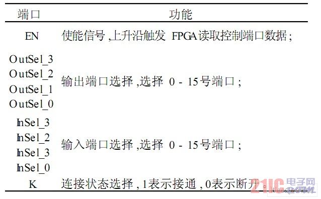
The output of the module is 16 sets of 16 bit parallel data, forming a matrix table. Each group of data represents an output port, each bit in the group represents a corresponding input port, and the elements in the table represent the connection relationship between the corresponding input and output, 0 means disconnected, 1 means connected.
In use, first select the input and output ports and the operating state that need to be operated, then input a high level to EN, trigger the control circuit to work, and connect or disconnect the selected input and output signals.
2. 3. 4 hybrid modules
The module consists of a data buffer register (AdderBuf) and an adder (Adder). The data buffer register reads the status of the control port (Sel) and then determines whether each input is valid, that is, whether it is sent to the output port. If an input port is valid, the port data is directly sent to the adder; if it is invalid, the data 0 is sent.
2. 3. 5 Switch Fabric Module
The working principle of the switch matrix is ​​a 16-to-256 splitter, which assigns each input to 16 channels and feeds them into the hybrid module of each output. Its structure is shown in Figure 6.
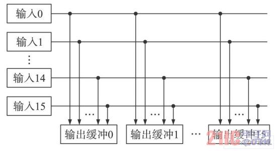
Figure 6 Schematic diagram of the switch fabric module.
2. 3. 6 output parallel/serial conversion module
This module is responsible for converting the 24-bit parallel data output by the hybrid module to the serial PCM code that the PCM1681 can receive. The data transfer format is the same as the PCM4204. A 24-bit shift register is built into the module to generate a serial output, and the parallel input is read according to the action of the channel clock (LRCK). The parallel/serial conversion process is shown in Figure 7.
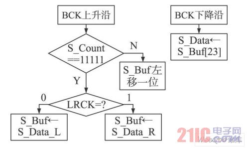
Figure 7 is a parallel/serial conversion flowchart.
3 system simulation and implementation
3. 1 System Simulation
The overall port and module block diagram of the FPGA is shown in Figure 8.
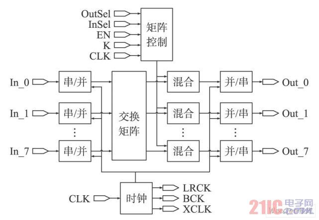
Figure 8 shows the overall port and module block diagram of the FPGA.
A 50 MHz clock signal is input from the clock input terminal (CLK); a control signal is sent to the switching control port to connect In_0 to Out_0, In_1 is connected to Out_1, ..., In_7 is connected to Out_7, and the control signal input is as shown in FIG.
Figure 9 Control signal input.
Input the hexadecimal serial data 000000 at the left channel input timing of the first serial signal input terminal (In_0), and enter the timing input 111111 at the right channel input input; similarly, input the timing input 222222 at the left channel of In_1, In the right channel input timing input 333333; ? In the left channel input timing input EEEEEE of In_7, input FFFFFF in the right channel input timing. Serial data input is shown in Figure 10.
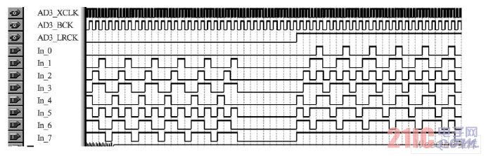
Figure 10 Serial data input.
The serial output of the system has corresponding data output. The output data of the left channel of Out_0 is 000000, the output data of the right channel is 111111, which is consistent with the input data of In_0; the output channel of Out_1 is 222222, and the output of right channel is 333333. , consistent with the input data of In_1; ?; Out_7 left channel output data EEEEEE, right channel output data FFFFFF, consistent with In _7 input data.
The serial data output is shown in Figure 11.
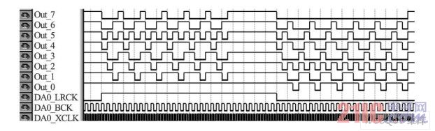
Figure 11 Serial data output.
Change the control port data so that the left channel input of In_1 (data 222222) and the right channel input of In _ 2 (data 555555) are connected to the left channel output of Out_0. As can be seen from Figure 3-5, the Out_0 serial data output becomes 777777. The serial data mixed output is shown in Figure 12.
From the above simulation results, the overall design of the FPGA can realize the exchange and mixing of serial digital audio signals to meet the expected design requirements.
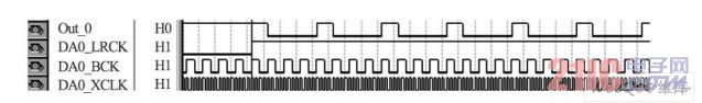
Figure 12 Serial data mixed output.
3. 2 system implementation
The physical picture of the exchange mixing matrix is ​​shown in Fig. 13.
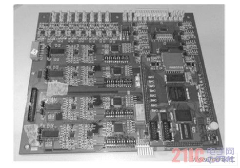
Figure 13 Exchange mixed matrix physical photos
In the physical test, the switched hybrid matrix is ​​first connected to the embedded control system, and the embedded control system is used to control it. Audio signals played by computers, MP3s, portable CD players, signal generators, etc. are used as input sources, and speakers, earphones, oscilloscopes, etc. are used as output devices to test switching, mixing and volume adjustment functions. After the * test, the output audio signal has no obvious distortion. Better signal quality is still guaranteed when multiple audio signals are mixed. The measured waveform of the input and output delay is shown in Figure 14, which is about 620 μs. The amplitude-frequency characteristic curve obtained by point-by-point measurement is shown in Fig. 15, and the passband is 20 Hz to 38.44 kHz.
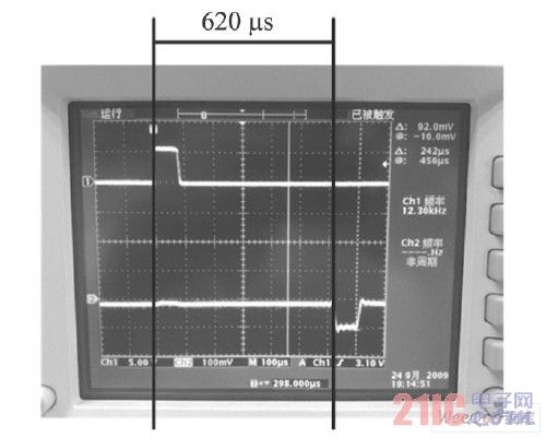
Figure 14 Input and output delay measurement waveform.
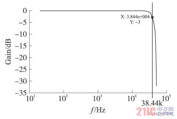
Figure 15 amplitude frequency characteristic curve.
The test results prove that the exchange hybrid matrix can correctly accept the commands of the control system, and complete the audio signal exchange, mixing and volume adjustment functions.
4 Conclusion
Aiming at the application requirements of audio switching system, this paper proposes a design scheme based on FPGA audio exchange hybrid matrix, and expounds and simulates the hardware and software design, and completes the physical production and testing.
The scheme described in this paper adopts FPGA as the core device of the exchange hybrid matrix, so it has strong versatility, and can reduce or increase the switching capacity, configure the sampling frequency of the audio signal and the sampling precision according to actual needs.
Through simulation and physical testing, FPGA-based audio exchange hybrid matrix can realize audio signal exchange, mixing and volume adjustment, and has the characteristics of low delay, high isolation and good sound quality, which can be applied to various conferences, command and communication. Such occasions.
Our company specializes in the production and sales of all kinds of terminals, copper terminals, nose wire ears, cold pressed terminals, copper joints, but also according to customer requirements for customization and production, our raw materials are produced and sold by ourselves, we have their own raw materials processing plant, high purity T2 copper, quality and quantity, come to me to order it!
Cable Terminals
Taixing Longyi Terminals Co.,Ltd. , https://www.longyicopperterminals.com