Both RF amplifiers in base stations and mobile phones require high linearity and high efficiency. By adopting some clever tricks, designers can take care of these two mutually exclusive requirements.
Key pointsThe new handset standard requires a linear RF amplifier.
Increasing linearity usually affects efficiency.
Digital predistortion is one way to achieve high linearity and high efficiency.
Doherty amplifiers implement a way to improve efficiency with hardware.
Nonlinear system modeling and simulation is difficult.
The mobile phone uses a modern modulation scheme that requires linear amplification of the RF signal. In order to achieve the required linearity, it is typical to consume more power at the output. This approach reduces efficiency, and efficiency is one of the most important parameters for cell phones, base stations or other electronic systems.
In the telecommunications field, mobile phones and base stations emphasize the need for efficiency. For mobile phones, efficiency directly affects the battery life. By increasing the efficiency of your phone, you can also extend the talk time, which is the most basic function for mobile phones. For the base station, high efficiency will reduce the electricity bill, and it is also important to reduce the heat. Reducing heat and power consumption produces a range of results that reduce initial investment, operating costs, and total cost of ownership.
In earlier cell phone modulation designs, the linearity of the output stage was not important because demodulation did not require the signal to be linear. CW (Continuous Wave), FM (Frequency Modulation) and GMSK (Gaussian Minimum Shift Keying) in GSM (Global System for Mobile Communications) communication technology all have a constant envelope and do not require linear amplification. New modulation techniques (such as EDGE, or enhanced data rate GSM evolution) require linear amplifiers. The linearity requirement can be achieved by underdrive the RF amplifier with sufficient difference between the output signal and the supply voltage. The problem with this method is that it directly reduces the efficiency of the amplifier.
When the output swing reaches the power supply level, the efficiency of the single transistor output stage increases. To increase efficiency, choose the appropriate supply voltage and load impedance to bring the output stage swing close to the power supply level. The average power consumed by the output transistor in this method is lower because the output transistor is always subjected to a lower voltage when the output signal is close to the supply voltage.
Unfortunately, driving the output signal close to the power supply level results in a linear degradation of the amplifier. Any amplifier, as long as its circuit design is such that its output swing is close to the power supply level, the linearity will be poor. The amplifier linearity problem is ultimately manifested in the form of amplifier clipping, limited by the supply voltage, and the signal change does not correctly represent the amplified input signal (Figure 1).
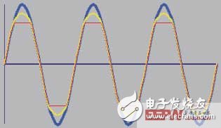
Figure 1. By comparing the blue input with the yellow moderately clipped waveform or the red severely clipped waveform, the clipping distortion can be clearly seen. Symmetrical harmonics similar to those in the figure appear as odd harmonics in the frequency domain. The amplifier nonlinearity produces distortion in the modulation that is harmonic-free with the two input tones.
Linear requirementsAlthough not easy to understand, linearity is not the main problem in many RF system designs. In fact, designers often use Class C amplifiers, which fully demonstrate that for certain types of communication signals, input sine waves are not necessarily the most critical requirement. This is the case, for example, for RF signals from FM stations. When transmitting a frequency modulated signal, the waveform zero crossing can include all information of the signal. Even if the peak is distorted, the demodulation signal fidelity will not be affected. Over-excited FM radio signals produce harmonics of the carrier frequency, which may be detrimental from an interference perspective, but the radio tuned to the over-excited FM radio signal still works (Figure 2).
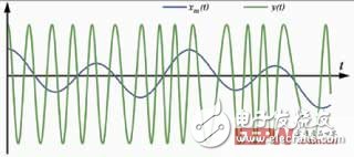
In Figure 2, the frequency modulated signal y(t) is unaffected by the amplifier nonlinearity. The information is contained in the zero crossings, not in the amplitude, so the amplifier amplitude distortion does not cause problems.
Over the past 10 years, the high cost of acquiring mobile radio frequency bands and the pursuit of revenue have prompted the design of advanced modulation schemes that can transmit more information in narrower frequency bands. A major advantage of these solutions is that they have higher bandwidth efficiency. Bandwidth efficiency is expressed in terms of megabits per megahertz or how many bits per Hz per second. The newly proposed mobile phone standard (such as EDGE) includes far more information than signal zero-crossing information. New handset modulation schemes (such as QAM, or quadrature amplitude modulation) carry information on both the phase and amplitude of the RF carrier frequency envelope signal. Take a look at the classic 64-QAM (64-state QAM) vector constellation (Figure 3). Both the signal phase and the amplitude use a series of symbol vectors to generate the envelope of the RF signal. Since there are 64 vectors, the information carried by any vector can represent 6-bit digital information, which makes the 64-QAM scheme have higher bandwidth efficiency, reaching 6 Mbps/MHz.
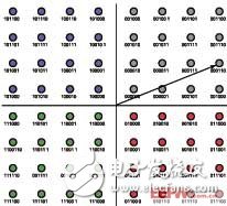
Figure 3. 64-QAM constellation map Each symbol vector can encode 6-bit data. Some vectors are prone to phase errors, and some vectors are prone to amplitude errors. In both cases, the accuracy of the waveform envelope is important, which makes the amplifier linearity problem very important.
In such advanced modulation schemes, linearity differences can cause problems. Since the amplitude and phase of the signal required by the demodulator are accurate, the instantaneous accuracy of the signal is very important; in FM transmission, only the zero crossing is meaningful. If the operating signal energizes the RF power amplifier to near the output level, the transistor will saturate, adding its inherent logarithmic nonlinear component to the signal. As a result, the symbol vector encoded by the amplifier discards the correct amplitude and phase. Nonlinear problems are severe enough to cause symbols to overlap and cause information loss.
Some solutions can solve the inherent nonlinearity of the transistor, but the transistor will be biased at the operating point of the transistor logarithmic transfer function. Therefore, it is more difficult to implement such a demodulation scheme. In addition, when the transistor output is close to the power supply level, the saturation of the transistor is difficult to estimate and process in the demodulation scheme because the supply voltage of each RF source has some uncertainty. The only way to solve the problem of poor symbol accuracy is to improve the accuracy of the RF power amplifier.
Due to the characteristic curve of the transistor, the Class A output stage has inherent nonlinear characteristics that make the output signal positive and negative amplitude asymmetry. At lower frequencies, nonlinear problems can be solved by feedback. Soon, transistor amplifiers evolved into op amps with forward gains of more than 120dB, allowing designers to improve signal linearity by using large amounts of negative feedback. This feedback is combined with the Class AB output stage for higher linearity. For example, National Semiconductor's LME49710 nominal linearity is 0.00003%. Note, however, that this linearity specification corresponds to a relatively low frequency operating condition. All amplifiers experience a drop in gain as the frequency increases. The current feedback amplifier structure has a small gain loss at high frequencies, but the gain is still reduced at high frequencies.
Keep in mind that the linearity improved by using large feedback is also related to the large forward gain. Since the amplifier has a low forward gain at high frequencies, the feedback is also small at high frequencies. Therefore, RF amplifiers, especially RF power amplifiers, cannot use conventional feedback at operating frequencies of 1 GHz and higher.
Equally difficult is that most RF amplifiers are open circuited, which means they are prone to power supply rejection and output saturation issues. Since the RF amplifier operates at a frequency close to the high limit of the transistor, it cannot be made into a high gain operational amplifier in actual operation. At this point, RF amplifier designers still have to face all the difficulties that tube equipment designers have encountered decades ago.
In addition to facing linearity, amplifier designers need to face other factors that affect linearity, making RF amplifier design more difficult. For example, amplifiers produce memory effects during power-up and heating conditions, introducing nonlinearities that vary with time or data. The electronic memory effect is similar to the memory effect in an old-fashioned guitar tube amplifier. This type of old-fashioned amplifier is equipped with an inexpensive power supply system, usually an open-line power supply with a capacitor on the rectifier line of the tube. A high volume of gravity chords strongly excites the output stage and pulls the supply voltage down after the capacitor is discharged. After the large load has passed, the line will charge the capacitor to restore its voltage, but the process takes tens of milliseconds. A drop in the supply voltage can change the bias of the guitar amplifier output transistor, causing different "data-dependent" nonlinearities. The degree of nonlinearity depends on the condition of the previous signal. Similar phenomena are likely to occur with RF power amplifiers. Some data sequences may require the use of symbols that can strongly excite the amplifier. This condition affects the power supply and amplifier bias and produces time-dependent nonlinearities. This nonlinearity varies with the RF carrier modulation.
In addition to such electronic memory effects, amplifier designers must also handle thermal memory effects. The transfer functions of the thermal and cold transistors are different, which introduces time-dependent nonlinearities into the system. If the ambient temperature is high or the data flow causes the output stage temperature to rise, the nonlinearity exhibited by the transistor will be different from that at low temperatures. As more CMOS chips are integrated into the RF power amplifier, the problems caused by heat become more serious.
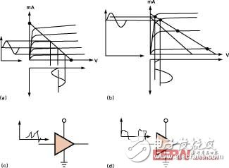
Figure 4. RF amplifier nonlinearity caused by transistor nonlinearity (a), clipping distortion (b) and electronic memory effect (c) and thermal memory effect (d).
Figure 4 shows the nonlinearity of the RF power stage. The core of transistor nonlinearity is that the transistor current-voltage transfer function is a one-to-one curve, not a straight line. The next question is how to solve the saturation problem when the transistor output voltage is close to the power supply level.
Method of increasing linearityRF designers can't just limit the amplifier's output swing to a small range while sacrificing efficiency. They can use feedback, feedforward and predistortion to maintain efficiency to extend battery life and save power. Feedback measures are for designs that require high linearity, narrow bandwidth, and moderate efficiency. Feedforward operation can be used in designs that require high linearity but wide bandwidth and low efficiency requirements. Pre-distortion can be used for medium linearity and bandwidth requirements, but can achieve high efficiency. Since the RF power amplifier operating frequency is so high, it is not practical to use conventional feedback measures. In this case, the term "feedback" usually refers to Cartesian feedback. In this type of feedback, the circuit re-converts the RF output back to baseband, obtaining I (phase) and Q (amplitude) signals, and sends these signals back to the input stage. This system can achieve high linearity, but only if the output stage is not over-excited. It will be less efficient than expected. Since the feedback amplifier is easy to oscillate, this method cannot be used for a wideband amplifier.
To achieve acceptable levels of linearity and bandwidth, RF designers have adopted a predistortion method: the modulated I and Q signals can compensate for the effects of deterministic system nonlinearities. Since digital systems can also use complex algorithms to predict thermal memory effects and electronic memory effects, such structures can remain linear in the event of such problems. Note that the inherent linearity of the components on the RF signal path is still involved here. There are limits to the correction in the digital domain. The closer the signal path is to the ideal, the easier it is for the digital system designer to provide an accurate predistortion signal.
James Wong, senior product marketing manager at Linear Technology, believes that designers are always clear about the inherent linearity of system components. “The active upconverter has built-in amplification compared to a passive upconverter followed by an amplifier, with low noise, good linearity and superior isolation, which gives it an excellent dynamic range.†He said, "This solution greatly reduces the difficulty for digital designers to provide signal pre-distortion." He pointed out that modern base stations also use Cartesian feedback. The circuit downconverts the signal and obtains the output signal I and Q components, which are then sent back to the DSP core. This approach allows the system to take complex algorithms with real-time Cartesian feedback and to take pre-distortion measures based on the components used in the signal chain (Figure 5).
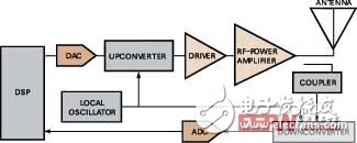
Figure 5 shows a mobile phone base station that takes digital predistortion measures based on the components used by the base station. Through Cartesian feedback, dynamic algorithms can also be used, which help compensate for the effects of memory effects and other nonlinear factors.
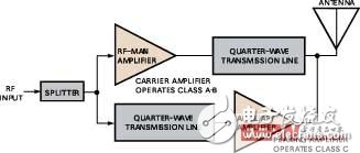
Figure 6. The Doherty RF amplifier uses an auxiliary amplifier to change the load impedance of the main amplifier for higher efficiency. This method allows the main amplifier to continuously output a large swing signal, reducing the power consumption of the amplifier. If the auxiliary amplifier reduces the main amplifier load impedance, the main amplifier outputs higher power.
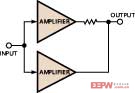
Figure 7. In this circuit, the same signal passes across the resistor and the apparent load on the upper amplifier is infinite. Both amplifiers drive the resistors at the same amplitude, so neither amplifier will output current or power to the resistor. If the phase difference of each amplifier signal is 180°, the characteristic resistance value of each amplifier is twice the resistance value. Doherty amplifiers use this principle to change the output and maintain high efficiency.
However, hardware designers do not have to use digital pre-distortion measures to improve linearity. Hardware can also play a role in improving linearity and efficiency; the better the inherent linearity of the component, the smaller the amount of correction for the digital system. Designers may consider using Doherty amplifiers. The amplifier was invented in 1936 by Bell Labs William H Doherty (Figure 6 and Reference 1). This amplifier has two RF paths. The RF signal is not only transmitted back and forth between the low power level and the high power level. The output voltage swing in the RF amplifier should be close to the power supply level. The Doherty amplifier uses an auxiliary amplifier to change the characteristic output impedance of the main amplifier. If the auxiliary amplifier produces the same signal at the other end of the transmission line, the output impedance of the amplifier that outputs the signal to the transmission line becomes infinite (Figure 7). Since both ends of the transmission line are of equal potential, no current flows and the power through the line is zero. If the auxiliary amplifier is not energized, the apparent output impedance of the main amplifier is the characteristic impedance of the transmission line. According to this principle, further, if the auxiliary amplifier is excited to have a phase difference of 180° from the main amplifier, the right side of the transmission line is differentially driven, and the characteristic impedance of the main amplifier is half of the impedance of the transmission line, so that the transmitted power is increased. The main amplifier output is always close to the output level. If the designer wants a lower transmit power, the auxiliary amplifier can increase the characteristic output impedance of the main amplifier, allowing the amplifier to output a smaller current at a voltage swing close to the output level, thereby outputting lower power.
The sophistication of the Doherty amplifier makes it suitable for the base station side of mobile applications. On the mobile phone side, the space and cost requirements are much stricter. In this case, the RF switch can be used to switch the gain block if necessary, thereby greatly reducing power consumption. For example, Avago's CoolPAM (Power Amplifier Module) RF components give handset designers an option to maintain high efficiency over a wide output power range (Figure 8). Instead of using a straight/direct converter to power the output stage, this straightforward technique can be used. The use of a converter allows the RF output stage to always operate close to the saturation point, thus improving efficiency. However, the direct/straight converter takes up a lot of space and has its own efficiency limit. Avago claims that using CoolPAM technology can extend talk time by more than an hour, making it an attractive option for mobile phone designers.

Figure 8. Low-cost handsets are suitable for direct efficiency to increase efficiency. Avago's amplifier modules switch between high power mode (a) with output power greater than 16dBm and low power mode (b) with output power less than 16dBm. The talk time can be extended by one hour due to improved efficiency.
ModelingThe pursuit of linearity and efficiency in RF power amplifiers has also had an impact on EDA tools used in RF system development. Because these RF systems are inherently non-linear, they also have all the same mathematical problems as other nonlinear systems. Spice and other circuit emulation techniques may not be applicable here and can be time consuming because RF designs typically require steady state operation. To reach this state, it may take billions of signal waves. RF designers typically use black box modeling methods (such as using S (scattering) parameters) to design the system. However, the S-parameter does not take into account nonlinear factors and lacks an amplifier offset model. In order to solve this problem, Agilent, which has promoted the S-parameter design method, recently introduced the X parameter, the multi-harmonic distortion model method (Reference 2). The response of the linear system response and nonlinear factors is integrated in the X parameters. Agilent has provided several articles detailing the technology, and will definitely add X-parameter simulation to Agilent's RF design tools in the future, and will certainly develop Agilent's test equipment that characterizes X-parameters.
Due to the design requirements of the new mobile phone modulation scheme, the design of the RF power amplifier is becoming more and more difficult. For a long time, the RF field has relied on sensory design and engineering experience. And because of the linearity and efficiency requirements of these new designs, people need more expertise to design a working amplifier. Design work has also begun to span different areas. RF, analog, and digital system designers all have an impact on signal chain performance. As experienced designers now have access to advanced tools and instrumentation from EDA and test equipment manufacturers, it is expected that performance will be even more dramatic in the future, while costs will be significantly reduced.
51V Battery Pack,Portable Battery Box,Portable Battery Bank,Ac Battery Pack
Zhejiang Casnovo Materials Co., Ltd. , https://www.casnovo-new-energy.com