The hardware platform and software design of an active phased array radar beam steering system are introduced.
l System principleIn order to reduce the circuit cost and increase the system reliability, the system adopts a centralized operation and distributed drive system with less equipment, convenient maintenance and high reliability. That is, the beam steering algorithm is implemented with a single board (called a computing board).
For the working mode, the computing board receives control commands from the radar console (including the azimuth and pitch increment codes of the main antenna, operating frequency, working mode code, etc.), and performs beam-control phase code calculation, transmission, distribution, and format rearrangement. . The computing board sends the processed serial beam control code through the driver to the beam steering component driver board of the array. The beam control component is further decoded, driven, and then sent to the component unit as a control code to implement the function of the beam steering system. The composition of the beam steering system is shown in Figure 1.
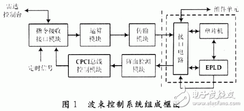
The phased array radar system requires the beam steering system to accurately and reliably control 512 antenna elements with a beam switching time of no more than 1 ms. Here are the key components needed to analyze the board. The computing board must complete the function of receiving commands, beam control algorithms and operation result transmission from the radar console within 500μs, and the FPGA device must be selected. The compensation data involved in the operation is one of the main objects of the operation. To be able to participate in the operation of the beam control algorithm in real time, it can also be updated online by the radar console, which requires the computing board to have a memory. The system uses a custom bus to receive radar control commands and information returned by the reporting front.
Regarding the hardware design of the driver board, not only the functions of driving, decoding, system self-checking, but also whether the control function of the driver board can be easily realized when the components are individually debugged. Due to the large number of devices, it is necessary to reduce the cost of equipment as much as possible on the basis of functions. Based on these needs, choose a single chip and a piece of EPLD. The hardware of the computing board shown in the left part of the dotted line in Figure 1 is composed. Among them, the radar console sends the beam control command, the received frame self-test and the detection information; the transmission module generates and transmits the serial beam control code, the clock and timing signals required for transmission.
The hardware component of the component driver board shown in the right part of the dotted line in Figure 1. The interface circuit receives the serial beam control code sent by the beam control computing board; the component unit receives the TTL level control code (including the transmit phase shift code, the receive phase shift code, the attenuation code, and the T/R switch control code). . The EPLD completes the decoding and control distribution code, and the SCU completes the functions of online self-test and offline control debugging. Control and debugging methods are more diverse and flexible than other provided system design methods.
3 software design3.1 computing board FPGA programming
The basic purpose of the wave control computing board is to meet the needs of the control of the array antenna unit. Here, the entire antenna front is equally divided into four sub-arrays. Each sub-array includes a&TImes; b antenna elements, as shown in Figure 2.
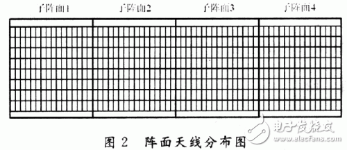
The antenna time division realizes two working modes of the full aperture SAR mode and the subaperture GMTI mode. When radar is detected by air or in the SAR mode, a full beam of the antenna is used to form a beam for transmission and reception. The physical center of the array is the coordinate origin of the array antenna unit. When the GMTI works, the whole array forms a single emission. The beam, while receiving, divides the four sub-arrays in azimuth to form four receiving beams. At this time, four coordinate systems are formed: the physical center of each sub-array is the coordinate origin of each array antenna unit.
According to the control requirements of the antenna unit, the two FPGAs are used here. The transmission uses four differential serial codes (two data codes, one address code, one 8 MHz clock code) to complete the beam of the array antenna unit. Control requirements. The logic functional block diagram of the FPGA internal program is shown in Figure 3. The serial port core, SRAM, and FIFO all call the resources inside the FPGA. The function of the serial port core is to receive control commands from the debugging computer during single-machine debugging and radar near-field testing of the beam steering computing board. SRAM is used to store the control code from the radar control computer when the radar is working in the front-end monitoring mode; the FIFO is used to store the result of the calculation of the operator (for debugging of the board of the computing board) or the self-test result of the component driver board. You can return to the debugging computer through the serial port to judge whether the intermediate result of the FPGA calculation or the final result sent is correct and whether the component unit and the corresponding signal path are good. The operation, transfer clock generation, and operation result transfer, read/write FLASH are all in the same state machine. The wave control computing state machine is shown in Figure 4.
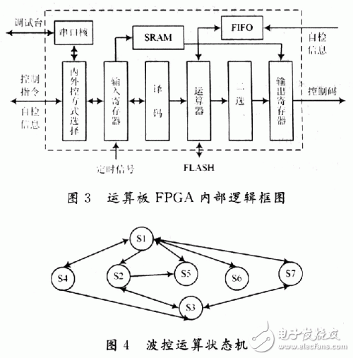
In Figure 4: S1 is the operation enable control and state transition condition control and variable initialization; S2 completes the beam control algorithm and arranges the calculation result according to the format; S3 generates the address and clock of the transmitted data and converts the parallel calculation result into a string S4 writes to FLASH; S5 reads FLASH; S6 writes to SRAM; S7 reads SRAM first, then posts in a predetermined format to jump into S3 state to transfer data from SRAM. The state transition condition of the state machine in S1 is the decoded control command from the radar console. The state machine will enter the corresponding state processing block according to different control commands.
Reloj Inteligente
Reloj Inteligente
everyone enjoys luck , https://www.eeluck.com