introduction
Since the outbreak of the energy crisis in the 1970s, people have come to realize that the world's energy is not inexhaustible. Therefore, how to apply scientific methods and combine production practices to design products with low energy consumption, high output and high efficiency has become the focus of practitioners. In this paper, the system design method for temperature detection and recording of metallurgical heating furnace temperature control system is given for the specific situation, in order to provide data basis for improving equipment performance, improve energy utilization and reduce production cost of products.
1 Detection system composition and function
1.1 Main components
The detector uses DSP (TMS320LF2407A) as the system's microcontroller to realize the functions of system signal acquisition, communication, human-machine interface and detection data storage (no loss of power loss). The biggest feature of this detector is that it can realize automatic signal acquisition and data storage of the system. Each data has its own time label, which can be used by users to query and count data at any time.
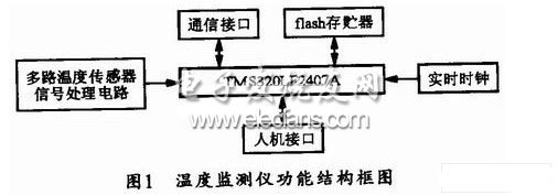
Figure 1 shows the functional block diagram of the temperature monitor. In the figure, the temperature monitor is divided into a microcontroller part, a human machine interface, a temperature sensor signal processing circuit, a memory, a real time clock, and a communication part.
1.2 Main functions
In order to adapt to the long working hours of the temperature control system, the system has large inertia and unattended characteristics. This automatic monitoring recorder system has the following functions:
The first is to accurately detect the 8-channel temperature value and automatically correct the detected value. The TMS320LF2407A control chip used by the monitor has abundant internal resources, and has 16 channels of 10-bit AD conversion channel, which greatly simplifies the system to external hardware. Expansion to improve system integration and reliability;
Secondly, the detector has real-time clock recording and data storage functions. The system uses Maxim's real-time clock chip to provide time stamps for the system's test data. The system periodically appends the data and attaches a clock mark, which is then stored in the memory for later recall and review at any time.
Third, the detector has a good human-machine interface. The human-machine interface of the system adopts a keyboard and a liquid crystal display, and can complete the input of the keys, the detection of each manual function, the display of various detection data, and the communication with the PC.
Finally, it is the communication function with the host PC. The detector performs necessary communication with the host computer through RS485 communication. When the host computer needs to call some data, the detector will locate the data and upload it immediately. At the same time, the communication mode also provides the possibility to realize the control of the DCS system. It can realize the DCS control network by multiple detectors and one industrial computer.
2 main hardware design
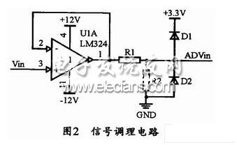
2.1 A / D front-end signal conditioning circuit
Because the signal from the thermocouple is a voltage signal of 0 to 5 V, and the A/D sampling signal range of the DSP can only be between 0 and 3.3 V. Therefore, the signal conditioning must be performed before input to the A/D circuit of the DSP. The conditioning circuit is shown in Figure 2. In the figure, the operational amplifier U1 constitutes a voltage follower, which can improve the driving ability and accuracy of the signal. R1, R2 can form a simple resistor divider network. The function of diodes D1 and D2 is to limit the clamp of the input voltage to the MD of the DSP. When the input A/D sampling voltage is higher than 3.3 V, the diode D1 is turned on, and the input voltage is always higher than 3.3 V. Similarly, when it is lower than OV, the diode D2 is turned on, and its input voltage is It must also be no lower than OV to limit the voltage input to AD to the allowed range.
2.2 Real-time clock interface circuit
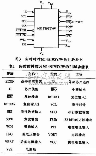
In order to enable the detector to automatically record data. The data collection time is provided for the user's reference. This system adopts the new real-time clock chip M14ST95Y/W produced by Maxim, and adopts SPI communication protocol to reduce the port resource occupation of the system. SPI communication only occupies the system SCL, SDI, SDO, chip select function E terminal and timing. Interrupt signal IRQ. Table 1 lists the pin functions of the M14ST95Y/W, Figure 3 shows the pin arrangement diagram, and the M14ST95Y/W integrates the clock crystal. At the same time, the voltage comparator with low voltage protection function, when the system power supply voltage is in the low voltage state (internal integrated 1.25V voltage comparator), the system will automatically transfer to the backup power supply, and start the write protection function in this state, Prevents the controller from erroneously modifying the real-time clock during undervoltage operation. In addition, the chip also has a watchdog real-time reset circuit. Therefore, this real-time clock chip is rich in resources, powerful, and requires fewer external components, which can improve the reliability of the system.
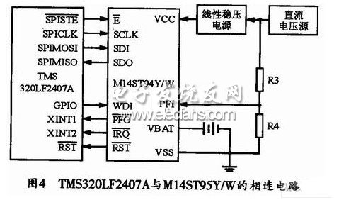
The connection diagram between the DSP and the real-time clock chip in this detector is shown in Figure 4.
Superfast Recovery Rectifier is the most popular use for diodes. Fast rectifiers convert alternating current (AC) to direct current (DC). They only allow one-way flow of electrons. Rectifiers have many uses and are often found serving as components of high-voltage direct current power transmission systems and DC power supplies. Fast rectifier diodes feature very low reverse recovery time, very low switching losses and low noise turn-off switching.

Super Fast Rectifiers,Fast Recovery Rectifiers,Super Fast Recovery Rectifier,Ultra Fast Rectifier Diodes
Changzhou Changyuan Electronic Co., Ltd. , https://www.cydiode.com