Design of wireless receiver based on AD9640
In the actual production of the wireless receiver RF front-end hardware, the design considerations such as the selection of the intermediate frequency, the center frequency and 3dB bandwidth of the band-pass filter, and the use of external passive components all require careful planning with different system applications. And adjustments to achieve the specified performance at the appropriate cost. This article takes cognitive anti-jamming as the design goal, and mainly discusses one of the core components of the receiver link-high-performance ADC, and describes how they meet the demand for high performance. In addition, the design of the receiver system also includes the steps of device selection and design, overall layout and wiring, and debugging process.
ADC design
The radio frequency signal received by the antenna must be A / D digitized so that the subsequent digital processing chip can perform digital signal processing [1]. ADC affects the power consumption, operating frequency dynamic range, receiving bandwidth and overall cost of the receiver system, and its performance can also affect the design of the receiver structure. Ideally, data conversion is performed directly after the receiver's link antenna, and the ADC directly samples the RF signal, which largely bypasses the analog device. An important feature of the receiver architecture in this paper is to place the ADC as close as possible to the RF front end and directly digitize at a higher intermediate frequency. Therefore, A / D design is one of the cores of receiver design.
Select the optimal sampling frequency
If the low-pass filter that filters the sampled output signal can have a rectangular coefficient of 1, it is possible to select any frequency within the range of the sampling rate without aliasing (without considering the jitter of the sampling clock). But in fact, such a filter cannot be made, and even a low-pass filter with a rectangular coefficient close to 1 is difficult to realize. If the subsequent low-pass filter does not have spectral translation conversion in the transition band, even if the rectangular coefficient is larger, it will not change the spectral structure of the original signal, which means that the interval between the translation spectra should be as large as possible. For the non-aliasing sampling rate, it is not that the higher the frequency, the larger the interval, and the non-aliasing sampling rate with the largest spectral interval is the best in reducing the difficulty of designing the subsequent low-pass filter.
This article first discusses the relationship between the alias-free sampling rate and the shifted spectral interval, and then selects an optimal sampling frequency in combination with the scheme.
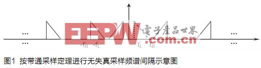
For the spectrum block shown by the dotted line in Figure 1, the left spacing is expressed as:
-fH + (m-1) fs- [fH- (m-1) fs] = 2 (m-1) fs-2fH (m = 1, 2, 3…)
The right spacing is expressed as:
fL-(-fL + mfs) =-mfs + 2fL
The condition for maximizing the spectral spacing is that the left spacing of the spectral blocks is equal to the right spacing:
2mfs-2fH = -mfs + 2fL
which is
![]()
For example, the signal received by the antenna is a signal with an intermediate frequency of 75MHz and a bandwidth of 1MHz, so the sampling frequency that maximizes the spectrum interval is: fs = 133.3333, 66.6667, 33.3333, 26.6667MHz ... (m = 1, 2, 3, 4 ...). Note that the maximum spectral interval referred to above is for the corresponding m. For different m, the absolute value of the interval decreases as m increases.
Since high-precision A / D devices over 100MHz are expensive, we choose m = 2, and the range of the distortion-free sampling frequency fs at this time is 50.3333MHz≤fs≤75.5100MHz. Also consider that a certain relationship must be satisfied between the sampling frequency of the ADC and the bandwidth of the IF filter:
fs≥B + B × w
Where w is the rectangular coefficient of the mid-band pass filter, this article is set as: w = 3. At this time, the aliasing of the ADC sampling passband will not occur, but the transition band will be aliased. The transition band will not alias until the ADC sampling frequency increases to twice the right side of the above formula. In essence, it will still "alias", but at this time the "aliasing" signal has been attenuated very weakly, for example, it is attenuated to more than 70dB smaller than the passband signal.
Finally, considering that the output rate of the subsequent DDC device after rate conversion is 8MHz (due to the ADC and subsequent algorithm processing requirements), the signal rate obtained by sampling is preferably an integer multiple of 2, while also considering the determination and control of the signal frequency band during sampling Convenient, the optimal sampling frequency is selected as 64MHz. The spectrum interval generated by this sampling frequency is also sufficient for subsequent filter design.
Device selection
Comprehensive sampling precision and rate requirements select the ADC: a 16-bit ADC can achieve a signal-to-noise ratio of approximately 96dB, but an ADC with an accuracy of 16 bits and a speed of more than 60 MHz is very expensive and difficult to purchase; a 14-bit ADC can A signal-to-noise ratio of about 84dB can also meet the requirements, and you can also buy faster products. This design selects 14-bit dual-channel A / D device AD9640 [2] for sampling. Its main performance is: selectable maximum sampling rate 80, 105, 125, 150MSPS; sampling precision 14 bits; spurious-free dynamic range 85dB @ 125MSPS; signal-to-noise ratio 71.8dB@125MSPS; low power consumption 750mW @ 125MSPS.
The sampling rate can be changed by changing the input clock, so that it can be extended by software without changing the hardware.
The "front end" or input configuration before designing a high-performance ADC is the key to obtaining the desired system performance. The optimization of the entire design [3] depends on many factors, including the characteristics of the application, the system division, and the architecture of the ADC. Many amplifiers are very suitable for the front-end circuit of high-speed ADC. ADA4937 can be used at frequencies below 150MHz; because it can handle a large output common-mode voltage range, its main advantage is that it is used in DC-coupled applications of ADCs. For narrow-band or resonant applications, match the output impedance of the filter and amplifier to eliminate the input capacitance of the ADC. A multi-pole filter is usually used to eliminate broadband noise outside the frequency range of interest.
Receiver PCB design
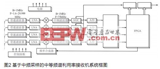
Based on the receiver block diagram of Figure 2 (DDC uses the four-channel digital downconverter AD6635 in the figure) and the basic requirements of PCB design, the overall requirements for the PCB layout of the receiver in this article can be proposed as follows:
â— All power supplies should leave a heat dissipation area on the top or / and bottom of the PCB [4];
â— The input and output interfaces of all boxes are located on the bottom layer of the PCB board;
â— Large areas of copper on the top and bottom of the PCB are grounded and grounded;
â— The power supply and its accessory components are close to each other and drive the power plane independently. The power plane is the power distribution network. The power supply of the components is obtained from the power plane, and it is filtered near the pins as needed;
â— All power cords enter the box and install "through-through capacitor";
â— The amplifier is directly grounded, and all high-gain amplifiers should be shielded to prevent them from oscillating.
ADC wiring
In the PCB schematic diagram, the network label of the analog ground is AGND, and the network label of the digital ground is GND. When connecting the analog ground and digital ground pins of the A / D converter together, most A / D converters connect the AGND and DGND pins to the same low impedance ground through the shortest lead. The external impedance of the DGND connection will couple more digital noise to the analog circuit inside the chip through the parasitic capacitance. Therefore, it is necessary to connect the AGND and DGND pins of the A / D converter to analog ground, but this method will cause problems such as whether the ground terminal of the digital signal decoupling capacitor should be connected to analog ground or digital ground.
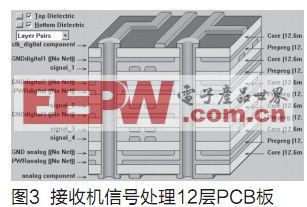
There are many A / D converters in the multi-channel receiver of this design. If the analog ground and the digital ground are connected together under each A / D converter, multi-point connection is generated, and the analog ground and the digital ground are connected. The separation between them is meaningless. If you do not connect in this way, you will violate the manufacturer's requirements. Therefore, the best way is to use a unified ground at the beginning, and divide the unified ground into an analog part and a digital part. This layout meets the requirements of ADC device manufacturers for low impedance connection of analog ground and digital ground pins, and at the same time does not form a loop antenna or dipole antenna and cause electromagnetic compatibility (EMC) problems. The PCB layout of AD9640 in this article is shown in Figure 3.
Receiver typesetting and wiring
In this design, the receiver wiring adheres to the 2W principle: the wiring width is W, and the line spacing is not less than 2W. The PCB circuit board is divided into two parts, the analog layer and the digital layer, with a total of 12 layers. The plate-making arrangement is shown in Figure 2. The wiring arrangement is designed as follows.
(1) Separation of analog / digital wiring and component layout. The high-speed signals are located in the high-quality wiring layers clk-digital component and signal_1. The high-speed signal lines are as far away as possible from the low-speed signal lines. The important low-speed signal lines are located in the low-speed signal layers signal_2 and signal_3. First, ensure that the key high-speed clock and signal lines are placed on the layers clk-digital component and signal_1; then ensure that the key low-speed signal lines are on the layers signal_2 and signal_3; Lines (especially clocks), high-speed signal lines entering low-speed wiring layers signal_2 and signal_3 should be far away from low-speed signal lines; finally, when the above principles cannot be implemented, wiring layers should be added.
(2) The lower three layers of the PCB board are analog circuits, and the upper seven layers are digital circuits; layer clk-digital component wiring 64MHz clock; layer signal_1 wiring 64MHz digital signals, including AD9640 sampling 64MHz high-speed digital signals; layer signal_2 and signal_3 wiring are less than 64MHz All other digital signals; connect the digital ground GNDdigital2 to GNDdigital1 with multiple vias. GNDdigital2 is only an isolation module for two systems to protect analog signals from digital interference. GNDdigital1 is used as the digital ground of the power supply + 5V; GNDdigital2 is used as the digital ground of + 1.8V, + 2.5V, and + 3.3V.
(3) All core components such as FPGA and voltage regulator are located on the top clk-digital component.
(4) Grounding method of copper plating on each layer:
â— Layer clk-digital component, signal_1, signal_2, signal_3 large area copper, and connected to GNDdigital1 through multiple vias;
◠Large area of ​​the analog component layer is copper-plated and connected to GND analog through multiple vias.
(5) Power supply wiring: The power supply line is filled in a large area according to the use area to form a divided power supply plane. The analog power plane PWRanalog is divided into two parts, 3.3V and 5V, and the digital power plane PWRdigital is divided into four parts, 1.8V, 2.5V, 3.3V, and 5V.
Physical manufacturing and testing
Figure 4 shows the physical picture of the designed receiver, and it is placed under a certain temperature, humidity and vibration pressure to test to check any design or work defects.
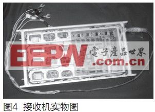
In the debugging process of the receiver designed in this article, the instruments used are: digital interface (Agilent N5102A), vector signal source (Agilent E8267D), microwave vector analyzer (Agilent 89650A), oscilloscope (Tektronix TDS 3032B), vector signal analyzer (Agilent 89611A), logic analyzer (Agilent 16900A). Figure 5 shows the connection diagram of the above instrument to the receiver test.
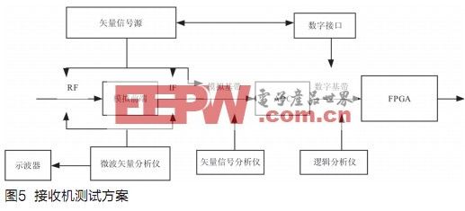
The vector signal source generates various modulation signals required by the receiver and inputs it to the RF front-end. After testing, the receiver is small, stable, and easy to debug. The actual ADC sampling rate is 63.488MHz; the FPGA data rate is 7.936MHz; The main clock rate of FPGA processing is 63.488MHz; the average bit error rate of communication signals with a bandwidth of 2 ~ 30MHz and -113dBm ~ -36dBm is received: Pe <10-5. Therefore, the radio frequency front end of this receiver has strong anti-interference and good electromagnetic compatibility, which meets the design requirements.
Solar Folding Bag,Flexible Foldable Solar Panels,Solar Flexible Panel,Flexible Portable Solar Panels
Shengtian New Energy (Shenzhen)Â Co., Ltd. , https://www.stenergysolar.com