TI's DS90UB964-Q1 is a multi-function camera hub that can receive serial camera data from four independent video streams via the FPD-Link III interface, and can be received from 100 when combined with the DS90UB913A/913Q serializer. Megapixel image Sensor data and support 720p/800p/960p resolution at 30Hz or 60Hz frame rate, mainly used in automotive ADAS systems such as surround vision systems, camera surveillance systems, sensor fusion and security and surveillance systems. This article describes the DS90UB964 -Q1 main features, functional block diagram, application circuit block diagram and evaluation module DS90UB96X-Q1EVM main features, circuit diagram, bill of materials and PCB design.
The DS90UB964-Q1 is a versaTIle camera hubcapable of connecTIng serialized camera datareceived from 4 independent video datastreams viaan FPD-Link III interface. When coupled with DS90UB913AQ/913Q/933Q serializers, theDS90UB964-Q1 receives data from 1-Megapixelimage sensors supporTIng 720p/800p/ 960p resolutionat 30-Hz or 60-Hz frame rates. Data is received and aggregated into a MIPI CSI-2 compliant output forinterconnect to a downstream processor. A secondMIPI CSI-2 output port is available to provide additional bandwidth, or offers a second replicatedoutput.
The DS90UB964-Q1 includes 4 FPD-Link IIIdeserializers, each enabling a connection via costeffective50-Ω single-ended coaxial or 100-Ωdifferential STP cables. The receive equalizerautomatically adapts to compensate for cable losscharacteristics, including degradation over time.
Each of the FPD-Link III interfaces also includes aseparate low latency bi-directional control channel that conveys control information from an I2C port andis independent of video blanking period. General purpose I/O signals such as those required forcamera synchronization and functional safetyfeatures also make use of This bi-directional control channel.
Main features of DS90UB964-Q1:
1• Qualified for Automotive Applications
• AEC-Q100 Qualified With the Following Results:
– Device Temperature Grade 2: –40°Cto +105°C
Ambient Operating Temperature Range
– Device HBM ESD Classification Level ±4 kV
– Device CDM ESD Classification Level C6
• Aggregates Data From up to 4 Cameras OverFPD-Link III Interface
• Supports 1-Megapixel Sensors With HD720p/800p/960p Resolution at 30-Hz or 60-Hz
Frame Rate
• Multi-Camera Synchronization
• MIPI DPHY Version 1.2 / CSI-2 Version 1.3Compliant
– 2× CSI-2 Output Ports
– Supports 1, 2, 3, 4 Data Lanes per CSI-2 port
– CSI-2 Data Rate Scalable for 400 Mbps / 800Mbps / 1.5 Gbps / 1.6 Gbps each Data Lane
– Programmable Data Types
– Four Virtual Channels
– ECC and CRC Generation
• Supports Single-Ended Coaxial or ShieldedTwisted-Pair (STP) Cable
• Adaptive Receive Equalization
• I2C With Fast-Mode Plus up to 1 Mbps
• Flexible GPIOs for Camera Sync and FunctionalSafety
• Compatible With DS90UB913AQ/913Q/933QSerializers
• CRC protection on the internal Data Path
• ISO 10605 and IEC 61000-4-2 ESD Compliant
DS90UB964-Q1 application:
• Automotive ADAS
– Surround View Systems
– Camera Monitoring Systems
– Sensor Fusion
• Security and Surveillance
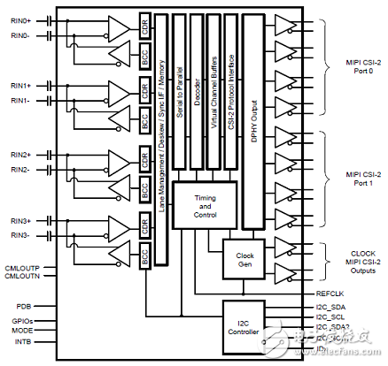
Figure 1. Functional Block Diagram of the DS90UB964-Q1
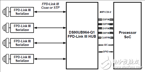
Figure 2. Typical application circuit block diagram for the DS90UB964-Q1
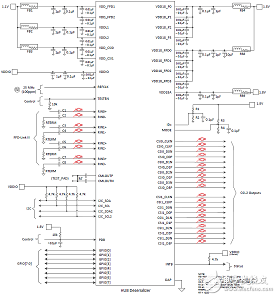
Figure 3. Typical connection diagram for DS90UB964-Q1 (coaxial)
Evaluation Module DS90UB96X-Q1EVM
The Texas Instruments DS90UB96X-Q1EVM evaluation module (EVM) is a functional board design forevaluating the FPD-Link III Deserializer to MIPI CSI-2 ADAS (Advanced Driver Assistance Systems) Hub.
This kit will demonstrate the functionality and operation of the DS90UB96X-Q1 family of chipsets. Theinformation provided in this document can be applied to devices such as DS90UB964-Q1. This EVM canalso be used as a hardware reference design for any implementation of the DS90UB96X- Q1 series. Someportions and components in the EVM or in this document may include the references to DS90UB964-Q1instead of addressing all part numbers. For the purposes of this document, the DS90UB964-Q1 is interchangeable with the DS90UB96X-Q1.
The DS90UB96X-Q1 is a versatile camera hub capable of connecting serialized camera data received from up to 4 independent video datastreams via an FPD-Link III interface using standard coaxial cables.When coupled with DS90UB913A/913Q serializers, the DS90UB964-Q1 receives data from 1 -Megapixelimagers supporting HD 720p/800p/960p resolution at 30/60Hz frame rates. The DS90UB96X-Q1 merges and manages multiple data streams into a MIPI CSI-2 compliant output for interconnect to a downstreamprocessor.
The EVM is a development add-on module to add surround view capability to any of a variety of videoprocessor systems such as the TI TDA3x ADAS Processor, or an Applications Processor, Image SignalProcessor (ISP), and SOC. The system consists of four cameras Each of which receives controlinformation and power through FAKRA coaxial cables, and uses the same cable to return the videoinformation to an EVM board. Each of the FPD-Link III interfaces also includes a separate low latency bidirectional control channel that conveys control information from an I2C port General purpose I/O signalssuch as those required for camera synchronization and functional safety features also make use of this bidirectionalcontrol channel.
The Texas Instruments DS90UB96X-Q1EVM helps to evaluate the operation and performance of theDS90UB964-Q1 and is available for order in two variants.
Key features of the evaluation module DS90UB96X-Q1EVM:
• Aggregates data from up to 4 cameras over FPD-Link III interface
• Supports 1-Megapixel sensors with HD 720P/800P/960P resolution at 30/60Hz frame rate (paired w/DS90UB913A)
• Multi-camera synchronization
• Supports MIPI DPHY 1.2/CSI-2 Version 1.3 compliant
– 2x CSI-2 output ports
– Supports 1, 2, 3, 4 data lanes per CSI-2 port
– CSI-2 data rate scalable for 400 Mbps/800 Mbps/1.6 Gbps per data lane
– Programmable data types
– Four Virtual Channels
– ECC and CRC generation
• Supports Single-ended Coax cable and Power Over Coax
• Adaptive receive equalization
• I2C with Fast-mode Plus up to 1 Mbps
• Flexible GPIOs for camera sync and functional safety
• Single +12V power supply for EVM
Evaluation module DS90UB96X-Q1EVM main components:
• DS90UB964-Q1
• On-board Power-over-Coax (POC) interface
• Four Fakra coax connectors for digital video, power, control and diagnostics
• Samtec QSH type connectors on CSI-2 interfaces
• On-board I2C programming interface
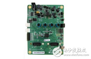
Figure 4. Outline of the evaluation module DS90UB96X-Q1EVM
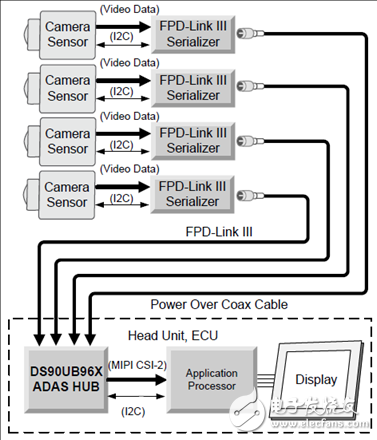
Figure 5. Typical configuration diagram of the evaluation module DS90UB96X-Q1EVM
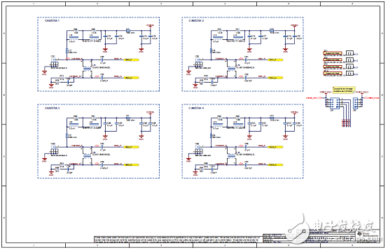
Figure 6. Circuit diagram of the evaluation module DS90UB96X-Q1EVM (1)

Figure 7. Circuit diagram of the evaluation module DS90UB96X-Q1EVM (2)
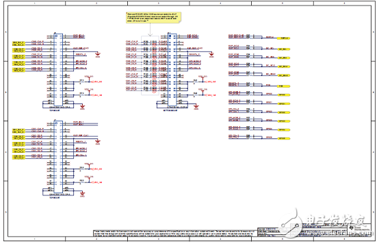
Figure 8. Evaluation module DS90UB96X-Q1EVM circuit diagram (3)
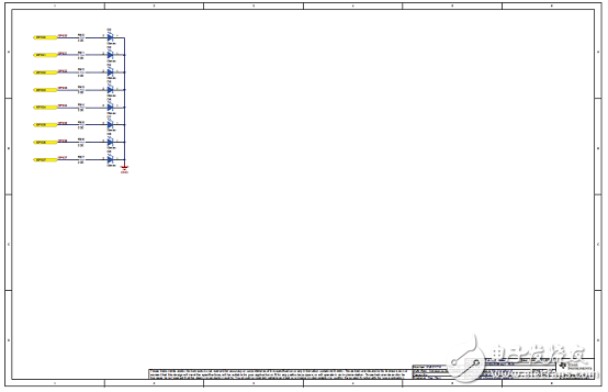
Figure 9. Evaluation Module DS90UB96X-Q1EVM Circuit Diagram (4)
Figure 10. Circuit diagram of the evaluation module DS90UB96X-Q1EVM (5)
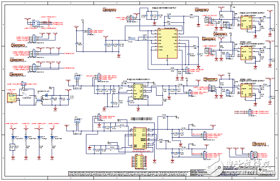
Figure 11. Circuit diagram of the evaluation module DS90UB96X-Q1EVM (6)
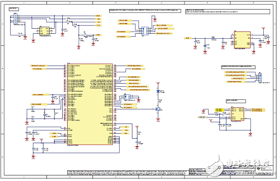
Figure 12. Circuit diagram of the evaluation module DS90UB96X-Q1EVM (7)
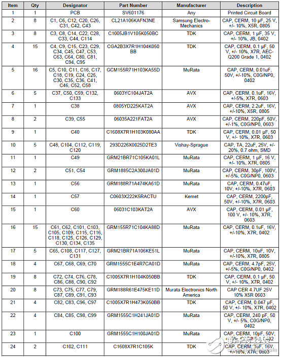
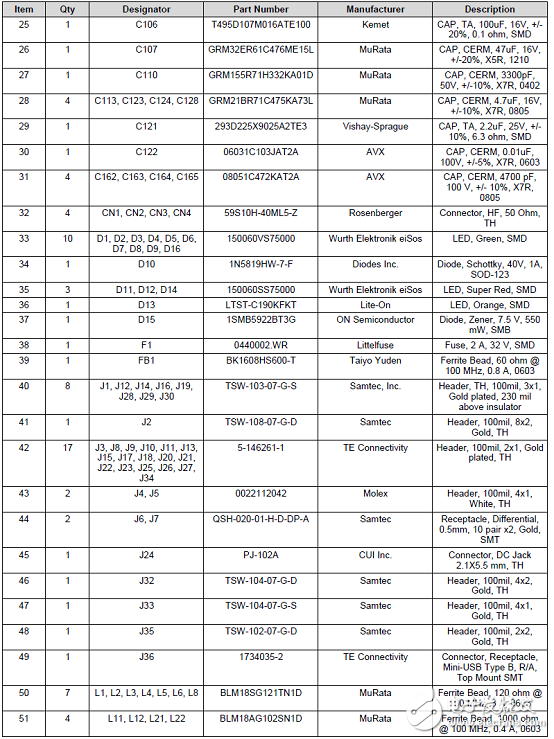
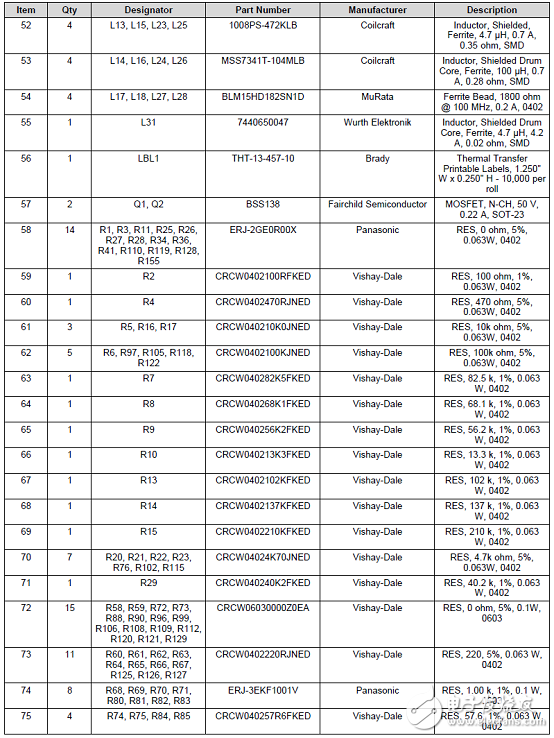
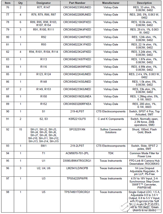
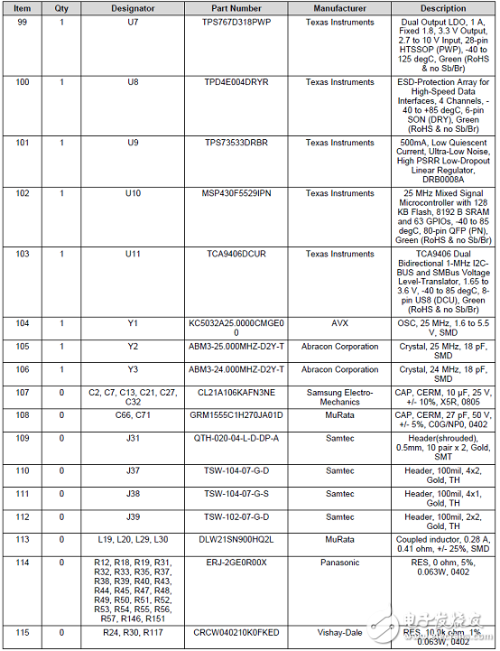
List of materials for the evaluation module DS90UB96X-Q1EVM equipped with SV601176-001:
List of materials for the evaluation module DS90UB96X-Q1EVM equipped with SV601176-002:
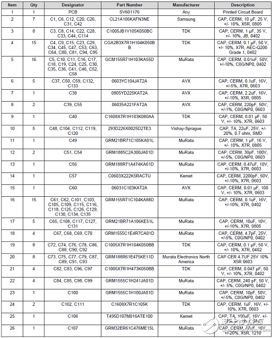
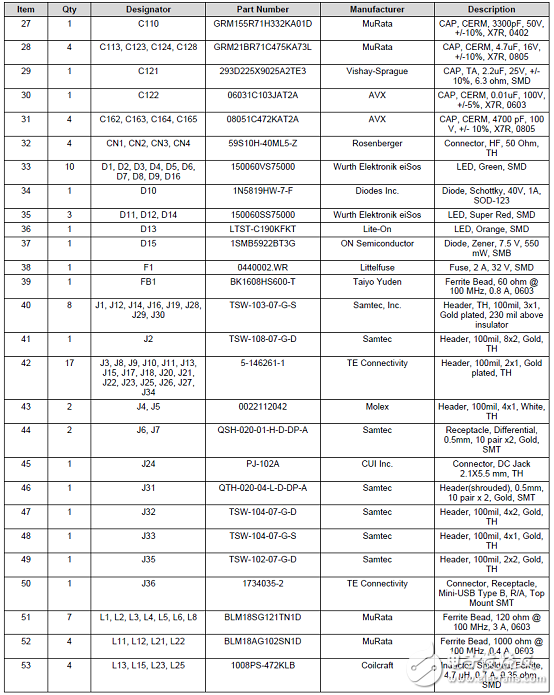
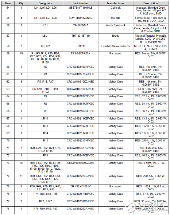
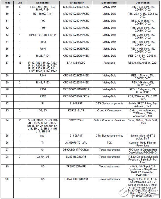

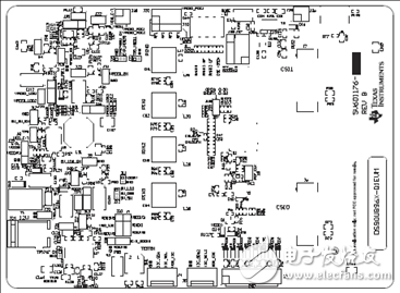
Figure 13. Evaluation Module DS90UB96X-Q1EVM PCB Design (Top)
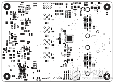
Figure 14. Evaluation Module DS90UB96X-Q1EVM PCB Design (Top Solder Diagram)
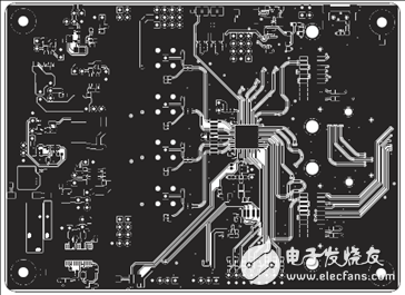
Figure 15. Evaluation Module DS90UB96X-Q1EVM PCB Design (Top 1)
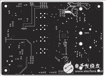
Figure 16. Evaluation Module DS90UB96X-Q1EVM PCB Design (Layer 2)
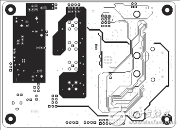
Figure 17. Evaluation Module DS90UB96X-Q1EVM PCB Design (Layer 3)
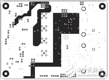
Figure 18. Evaluation Module DS90UB96X-Q1EVM PCB Design (Layer 4)
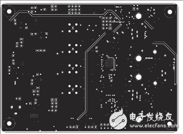
Figure 19. Evaluation Module DS90UB96X-Q1EVM PCB Design (Layer 5)
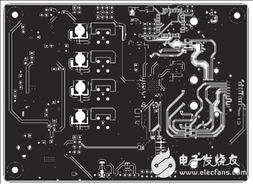
Figure 20. Evaluation Module DS90UB96X-Q1EVM PCB Design (Lower Level 6)
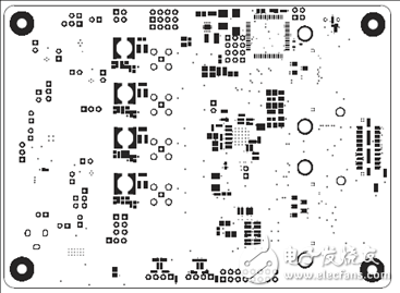
Figure 21. Evaluation Module DS90UB96X-Q1EVM PCB Design (Bottom Soldering Diagram)
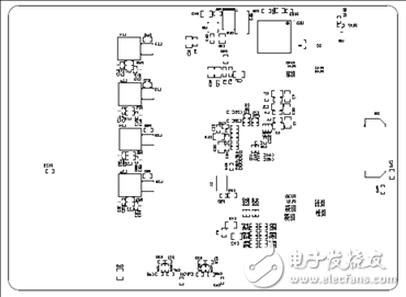
Figure 22. Evaluation Module DS90UB96X-Q1EVM PCB Design (Bottom)
Basic Physics Experiment Instrument Series
Basic physics experiment instrument series, used in physics laboratories of colleges and universities.
Basic Physics Experiment Instrument,Light And Optical Instruments,Optical Viewing Instrument,Microscope Light Source Instrument
Yuheng Optics Co., Ltd.(Changchun) , https://www.yuhengcoder.com