I originally thought about writing the time after the two blog posts of GTX, but I have been busy recently. I have been taking the image processing AXI framework and the FPGA-DSP dual platform board. Let's share the debugging experience with you.
Recently debugging a new ArTIx7 board, I encountered a very strange problem. The problem is that the FPGA can use the JTAG port to transfer the program to the FPGA, and the FPGA can also run. When the configuration mode selects MASTER SPI, it can also be downloaded through the JTAG port. Succeeded, but the problem is that the FPGA can not read the FLASH configuration file after power-on, which causes the FPGA to fail to start in Master SPI mode. After 2 days of troubleshooting, the M1 and M2 mode selection pins on the configuration circuit are finally located. The pull-down resistor is incorrect. The 10K resistor pull-down is used on the hardware, which causes the Sample Mode Pins process in the FPGA startup process (shown in Figure 1 of the xilinx FPGA) to be faulty. The factual basis is shown in Figure 2.
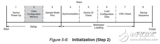
figure 1
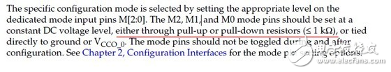
figure 2
The official statement is to connect directly to VCC or GND. If the pull-down resistor is connected, the resistance should be less than 1K. Use a universal meter to measure the voltage values ​​of M1 and M2. It is found that the value of the voltage is about 1.3V in the case of 10K pull-down. In order to get into the reasons for this situation, go to the official manual and finally find a sentence in UG470, as shown in Figure 3.
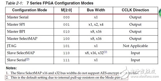
image 3
It turns out that the MODE PIN has an internal pull-up resistor, which explains why using a multimeter to measure M1 and M2 will have a voltage of about 1.3V.
So how can such problems be quickly found out? In fact, the information provided by IMPACT is very useful. This tool can help hardware personnel to provide a lot of information in the early debugging of the board, especially the internal voltage and internal startup status register. How to go To see this information, first power on the board, then open the IMPACT-Boundary Scan-IniTIalize chain, after scanning the device, open the menu bar - Debug-Read Device Status, as shown in Figure 4.
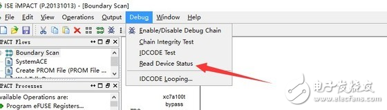
Figure 4
After selecting the read device status, you can see that the console prints the following information, as shown in Figure 5 and Figure 6.
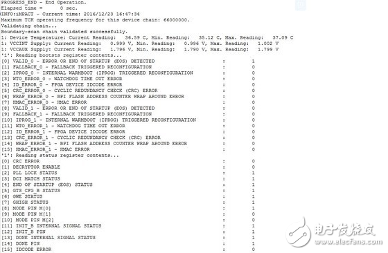
Figure 5
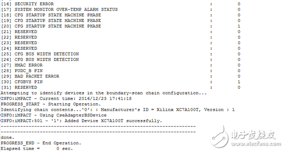
Figure 6
From the information printed by the console, you can see the temperature of the chip, the voltage value of the core VCCINT and the voltage value of the VCCAUX, the value of the status register of the FPGA, and the value of the configuration pin. This information can help the engineer conveniently. The FPGA temperature, internal voltage, startup state, and related configuration pins are judged to accelerate the positioning problem.
Membrane Switch Assemblies,Lcd Display Membrane Switch,Tactile Membrane Switch Keypad,Overlay Tactile Membrane Switch
KEDA MEMBRANE TECHNOLOGY CO., LTD , https://www.kedamembrane.com