Core Tip : The thin design of the smartphone makes the touch panel controller vulnerable to noise generated by the display. To solve this problem, touch chip developers have begun to improve the design of touch sensors and enhance the synchronization of the operating frequency of touch modules and LCD panels. At present, the new design method has been imported by In-cell embedded capacitive touch screen developers.
The noise generated by the display will interfere with the sensing function of the capacitive touch screen. To further improve, it is necessary to understand the basic principles of liquid crystal display (LCD) technology and the causes of noise, in order to find out the way.
First of all, it is necessary to sort out what kinds of displays appear on the market today, such as active matrix organic light emitting diode (AMOLED), thin film transistor (TFT) LCD and other smart phones. In general, the quality of AMOLED is better, and the noise generated by the touch chip is less than that of the LCD. However, the AMOLED panel is more expensive and more difficult to manufacture than the LCD; therefore, the LCD still dominates the entire market. Since LCD displays are the most popular technology, they generate the most noise, so this article will focus on the LCD.
Thin touches increase LCD noise
In order to understand how the LCD generates noise, it is necessary to master the basic operation principle of the LCD. As shown in Figure 1, from the bottom of the LCD display, the light is reflected and then reflected upward. Each pixel contains three sub-pixels of red, green and blue, and each sub-pixel contains a liquid crystal layer (Sandwich). The top of the laminate is laminated with an indium tin oxide (ITO) transparent conductive film with a liquid crystal material sandwiched between the top layer and the bottom layer.
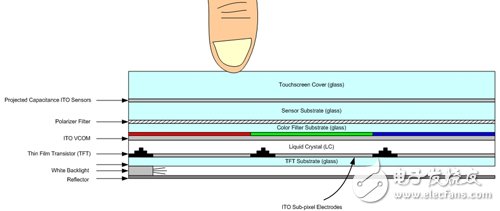
Figure 1 LCD and touch panel architecture
The top layer is the common pole of all sub-pixels, usually called the VCOM layer; the bottom layer is specially configured for the sub-pixels, called the sub-pixel electrode. When the voltage is conducted to the LC stack, the liquid crystal material will reverse the polarity of the white light ( Polarity), a polarizer above the stack that only passes light of a specific polarity. If the polarity of the light is the same as the polarity of the polarizing plate, the sub-pixel will reach the highest brightness. If the polarity of the light is opposite to that of the polarizer, the brightness of the sub-pixels is minimized.
In addition, each sub-pixel has a color filter (R, G, or B) that acts like a stained-glass window. By directing the voltage to the liquid crystal stack of three sub-pixels, the pixel can be set to any RGB. Composition color. Each sub-pixel also contains a TFT as an on/off switch that leads to the voltage of the LCD stack. This design effectively sorts the pixels on the screen when refreshing the full-screen image.
As shown in Fig. 2, the pixel is turned on at the gate of the TFT, the source of the TFT is connected to the output of the color digital analog converter (DAC), and the drain of the TFT is connected to the ITO sub-pixel electrode. Since the liquid crystal material cannot withstand direct current (DC) voltage, the bias voltage must be alternating current. There are also differences between ACVCOM and DCVCOM. The former mainly drives VCOM and sub-pixel electrodes through a differential voltage. Because the VCOM layer is driven by AC, it is called ACVCOM. The latter drives the common pole layer through DC, while the sub-pixel is driven by AC. This signal is yawed with the DC value as the center. The two VCOM squares have different performance and cost advantages and disadvantages.
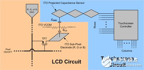
Figure 2 LCD and touch panel circuit diagram
The industry knows that ACVCOM will generate a lot of noise due to the active driving of a large area of ​​ITO (VCOM) layer; DCVCOM is well known in the industry for its low noise performance, but this is not necessarily the case. In the past, there was a thin gap (Air Gap) between the sensor and the LCD surface. However, today's mobile phones are made thinner, so most of them no longer have this layer of voids. The way to directly attach the ITO sensor to the LCD surface is gradually adopted by most manufacturers, resulting in more serious noise coupling.
What's more, the current design direction of the industry requires that the touch panel controller can directly sense VCOM and sub-pixel electrodes, that is, in-cell (In-Cell) touch technology. Therefore, between the touch screen and the LCD controller. Synchronization can eliminate noise interference when scanning the touch screen; now most LCDs of smart phones are gradually phasing out ACVCOM, switching to higher quality DCVCOM and AMOLED displays, and moving towards direct fit or In-Cell, thereby reducing Manufacturing cost and product thickness.
LCD noise will be coupled to the touch sensor
As for how LCD noise is coupled to the touch screen sensor, mainly its circuit noise will be coupled to the two capacitors of the touch screen circuit. The first capacitor is CLC, which is formed between the sub-pixel and the VCOM surface, during which the liquid crystal material acts as a dielectric.
In the case of a DCVCOM display, the AC signal that drives the subpixels is coupled to the VCOM layer and becomes noise and passes to the entire panel. The DCVCOM layer appears to be a good AC ground because the node is maintained at DC voltage; in fact, the noise is weakened because the VCOM layer is made of ITO with relatively high resistance, and a second miscellaneous will occur here. The case of the coupling capacitor - CSNS.
The CSNS is formed between the VCOM layer and the capacitive sensor. The remaining noise voltage of the VCOM layer is coupled to the capacitive touch screen sensor through the CSNS and transmitted to the pin of the touch panel controller. For ACVCOM displays, since VCOM is driven in an AC mode, LCD noise is also directly coupled to the touch screen sensor via CSNS.
The method of measuring and analyzing LCD noise is quite simple. You can use a conductive metal to connect to the oscilloscope probe, or use a piece of copper that faces down and then directly cover the surface of the display (do not attach a touch screen sensor). Alternatively, a large copper plate or a piece of copper tape can be used, but it should be noted that the noise intensity will decrease as the conductor size shrinks, so it is better to cover the entire surface to minimize the coupling error of the oscilloscope.
Figure 3 shows the extracted ACVCOM signal waveform, which usually contains a high-intensity fundamental frequency whose waveform is close to a square wave. ACVCOM operating frequency is generally between 5k ~ 25kHz, usually the fundamental frequency will correspond to the speed of each column of the LCD update (scanning line frequency).
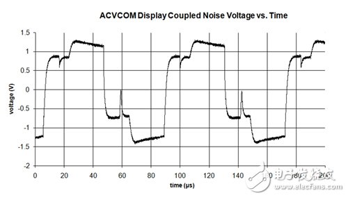
Figure 3 ACVCOM display coupled noise and time diagram
Figure 4 shows the actual captured DCVCOM waveform. The DCVCOM waveform is similar to several sharp high-frequency pulses. There is no high-intensity fundamental frequency similar to ACVCOM, but the harmonic amount can be easily increased to 50k~300kHz, and the short-term pulse corresponds to the sub-pixel driving signal. The characteristics of DCVCOM noise are highly dependent on the displayed image. The worst-case image is usually a black-and-white interlaced pixel arranged in a checkerboard pattern on the entire screen (it looks close to gray); however, before analyzing the DCVCOM display characteristics, be sure to test more Different images.
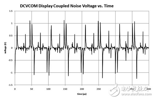
Figure 4 DCVCOM display coupled noise voltage and time diagram
Guang Er Zhong(Zhaoqing)Electronics Co., Ltd , https://www.gezadapter.com