1 Introduction
The embedded component substrate can reduce the size of the PCB or the module due to the three-dimensional arrangement of the components, shorten the connection path between the components, and reduce the transmission loss. It is a mounting technology that can realize the multifunctionalization and high performance of the portable electronic device. A buried component substrate in which an LSI or a passive component is embedded in a multilayer board has been used since 2003, and since 2006, it has been officially used as a high-function portable telephone or a small module substrate for use in a watch. These substrates use feature structures and processes developed by component manufacturers and PCB manufacturers, respectively. This article introduces the classification of the embedded component substrate technology embedded in the specifications of the Japan Electronic Circuit Industry Association (JPCA), the components used, the mounting techniques and evaluation analysis.
2 Classification of embedded component substrate technology
The embedded component substrate is roughly classified into a method of embedding an individually manufactured component and a method of forming a direct component on the substrate. I am limited to the technology of the former. Fig. 1 shows the classification of a buried type embedded component substrate in accordance with the manner in which the embedded component is mounted. The component mounting method on the PCB generally has two types of pad connection methods and via hole connection modes.
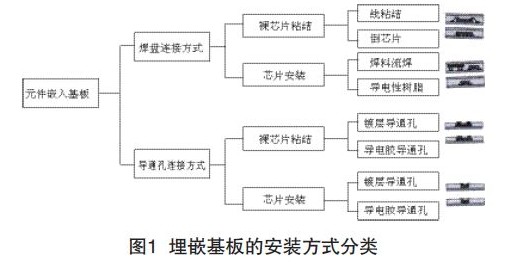
Fig. 2 shows a representative manufacturing process of the pad connection method and the via connection method.
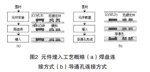
In the pad connection method, an embedded component is first mounted on an electrode formed on a substrate and electrically connected. After the connection is completed, the components and the electrodes are simultaneously filled and buried with an insulating resin. Use existing surface mount technology when connecting. The connecting material is made of solder or conductive paste. Installation of embedded components: Die bonding when the component is bare chip; Mounting when the component is passive component or molded package (Mould PACkage) or WLP (Wafer LevelChip Scale Package): bare chip Flip Chip Bond uses ultrasonic bonding, C4 (ControlLED Collapse Chip Connection), ESC (Epoxy Encapsulated Solder Connection), conductive resin and anisotropic conductive resin (ACF) Installation techniques such as /ACP, AuisotropIC ConducliveFilm /Anisoropic Conductive Paste) and non-conductive resin (NCF/NCP, Non Conductive Film / Non Condctive Paste). The passive components are connected by solder reflow or conductive resin. In the pad connection method, since the component connection uses the conventional surface mounting technology, it has the advantage of effectively utilizing the existing manufacturing equipment. In addition, since the inspection after the component mounting connection and the previous embedding is performed, it is possible to perform screening, repair, and rework of defective products occurring during the mounting process.
In the via connection mode, the PCB and the component are electrically connected before the component is embedded with an insulating resin. After the component is buried, the resin covering the electrode of the element is subjected to laser processing, and after the via hole is formed, the via hole is filled with a plating layer to electrically connect the PCB and the component. The via connection is characterized by bonding a direct copper (Cu) layer to the electrodes of the component. Since there is no joint such as solder or bump used in surface mounting, it is expected to have the same low connection resistance and high connection reliability as the internal wiring of the multilayer board, and a full-layer IVH (Interstitial Via Hole) can also be used. The conductive adhesive used is connected by a via hole, and the same conductive paste as the interlayer connection of the multilayer board is used for connection with the component, and the integrated lamination process of simultaneously embedding and connecting can simplify the complicated embedded component of the substrate. Manufacturing process.
The types and approximate manufacturing processes of the embedded component substrate classified according to the mounting technique of the embedded component are described above. Various mounting techniques employed in the manufacture of the embedded component substrate will be described below with reference to the development examples to date.
3 buried component substrate with pad connection
After the components are mounted on the inner substrate in the pad connection method, they are buried with an insulating resin. The embedded components are divided into bare chips (Bare Die) and other components. The surface mounting technology for connection is described below.
3.1 bare chip bonding method
Figure 3 shows the process of mounting an embedded bare chip using a flip chip.
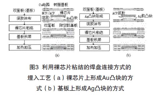
Fig. 3(a) shows the formation of gold (Au) stacked bumps on the electrodes of the bare chip. The method of heating and pressurizing the connection between the NCP and the electrode of the PCB. The surface of the electrode of the PCB is not plated with gold (Au) or tin (Sn), but the original copper (Cu). The copper (Cu) surface is roughened to improve adhesion to the resin. When the heating and pressurizing connection is made, the joint must maintain compressive stress, which is essential for improving the reliability of the connection. In Fig. 3(a), focusing on the thermomechanical properties of the NCP, a resin having a high elasticity and a high expansion coefficient can be selected to obtain a sufficiently practical connection reliability.
There is also a mounting method for the hot-press connection using ACP instead of NCP. After the gold (Au) ball bumps are formed on the aluminum (Al) electrode of the bare chip, the primer ACP is applied and pressurized heating is performed to electrically connect. Bonding reliability and NCP are also dependent on the physical properties of the primer resin. Figure 3(b) shows the connection using silver (Ag) glue bumps and ACP. Silver (Ag) paste is printed on the electrodes of the PCB to form silver (Ag) bumps, and the primer ACP is bonded by thermocompression using a flip chip bonder. Copper (Cu) or gold (Au) bumps are not formed on the electrodes of the bare chip, but aluminum (Al) is used for thermocompression bonding.
The bonding technique of the hot-press bonded silver (Ag) adhesive bump of Fig. 3(b) has been mass-produced in the laminated board, and the interlayer bonding technique using the conductive bump (B2it, Buried Bump Interconnection Technology) is applied. .
3(a) and 3(b) are practical ratios of the components embedded in the substrate in combination with the multilayer board manufacturing technology, and the interlayer connection is performed by using conductive bumps using the component connection technique of NCP and ACP. A double-panel connected by conductive resin bumps is mounted, and after the components are mounted on the inner layer, the outer layer substrate is combined with heat and pressure to embed the components, and the bumps are used to collectively connect the wiring layers. The process of forming a line before the component is buried is advantageous in reducing the defective rate and improving the productivity.
3.2 chip installation method
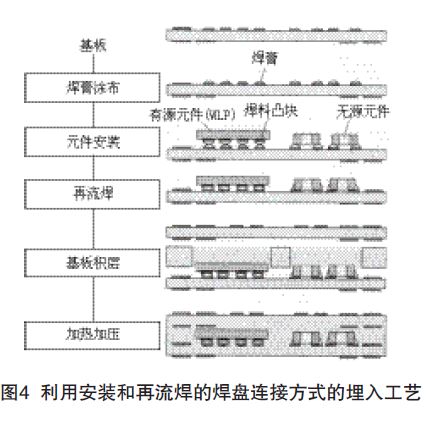
Fig. 4 shows a connection method in which a chip mounter (Chip Mouuter) is mounted on a substrate on which an inner layer of a solder paste is mounted, and a solder is melted by a reflow process. The active component and the passive component are mounted and connected simultaneously by chip mounting and reflow soldering processes for LSI WLP. It is an embedding technology that can be used by most common components such as LSIs or modules in model packaging. When soldering the embedded component, since the module substrate on which the component is mounted on the surface of the substrate is mounted on the mother board for the second time, it is feared that the solder bump (solder ball) melts and affects the conduction and insulation characteristics after the reflow soldering process. . Therefore, the resin is used to cover the periphery of the solder, and the flow generated by the remelting is suppressed, so that the above problem can be avoided.
4 via-hole connection device embedded substrate
In the via connection method, the device is connected to the substrate after being embedded. The electrodes of all the elements of the active element and the passive element are regarded as line patterns of the inner layer, and a wiring layer is formed on the upper portion of the element by a lamination technique.
4.1 bare chip bonding method
The embedded LSI WLP is made of copper (Cu) lines to extract WLP electrodes, which expands the inter-electrode pitch and realizes a high embedding process with the existing PCB processing technology. In addition, a good bare chip (KGD, Known GoodDie) is ensured due to WLP. It has great advantages over the via connection method in which the components are difficult to repair after connection.
Fig. 5 shows a manufacturing process of an active device embedding technique of a representative via connection. The embedded LSI is WLP-formed to form copper (Cu) lines and copper (Cu) bumps, and resin coating is applied. After attaching a bare die attach film (DAF, DieAttachment Film) to the back surface of the thinned bare chip, the positions are overlapped and bonded upward on the substrate. The prepreg and the surface layer are laminated, and the bare chip is embedded after heating and pressing. Laser processing is performed on the surface of the substrate at the electrode position of the embedded WLP, and after the via hole is formed, the via hole is filled with a plating layer to connect the electrode of the WLP and the wiring of the substrate. Since the surface of the bare chip is protected by a resin, it is possible to reduce the risk of damage or contamination in the embedded processing.
Suizhou simi intelligent technology development co., LTD , https://www.msmvape.com