1 high-speed SoC microcontroller C8051F040 features
The C8051F040 family of devices is a fully integrated mixed-signal, system-on-chip MCU with 64 digital I/O pins and an on-chip integrated CAN2.0B controller. Its main features are: (1) 8051-compatible CIP-51 core with high-speed pipeline structure (up to 25 MIPS); (2) Full-speed non-intrusive system debug interface (on-chip) 64 KB (C8051F040/1/2) /3/4/5) EEPROM, SMBus/I2C and two UARTs available in system-programmed flash memory, (4K+256)B on-chip RAM, 64 KB external data memory interface and hardware implementation Serial communication interface, on-chip integrated watchdog timer and VDD monitor and temperature sensor, C8051F04x series devices with clock oscillator, is a truly on-chip system that can work independently. All analog and digital peripherals can be enabled/disabled and configured by user firmware. Flash memory also has system reprogramming capabilities that can be used for non-volatile data storage and allows for field-updated 8051 firmware. Each MCU operates over the industrial temperature range (-45°C to +85°C) and operates from 2.7 V to 3.6 V. Port I/O, RST, and JTAG pins all allow an input signal voltage of 5 V.
2 LED  Hardware circuit and display working principle
2.1 driving method
When going to the LED When a forward voltage is applied to the device, the current flowing causes it to illuminate. Therefore, LED The drive problem translates into the problem of how to make the PN junction positively biased. In order to control its luminous intensity, the regulation of its forward current is also solved. The driving method is divided into DC drive, constant current drive and pulse drive.
2.1.1 DC drive
DC drive is the easiest way to drive. led Operating point by supply voltage, series resistor and LED The volt-ampere characteristics of the device are determined together. This drive is suitable for LED Less device and constant luminous intensity.
2.1.2 Constant current drive
led The forward characteristics of the device are steep, and the dispersion of the device makes the forward current of each device different under the same power supply voltage and the same current limiting resistor, thus causing a difference in luminous intensity. If the LED The device is driven by constant current, and as long as the constant current value is the same, the luminous intensity is relatively close. The output characteristics of the transistor have a constant current characteristic, so the transistor can be used to drive the LED .
2.1.3 Pulse Drive
Using the visual inertia of the human eye, using LED The device is repeatedly turned on and off to illuminate it, which is a pulse drive mode. Pulse drive is mainly used in both scanning drive and duty cycle drive. The main purpose of the scan driver is to save the drive and simplify the circuit. The purpose of duty cycle control is to adjust the illumination intensity of the device for grayscale control in image display. In practical applications, it is often used in combination.
2.1.4 common LED Display driver
At present, the serial control driving method is generally adopted, that is, the displayed data is sent to the point driving circuit through serial mode, and the 4953+74HC595 is used as the driving.
2.2 LED Hardware circuit introduction
256 B two-color LED The screen is mainly composed of 32 8×8 LEDs The module consists of 32 74HC595, 8 4953, 2 74HC245 and 2 74HC138. led The screen is divided into an interface circuit, a driving circuit, a decoding circuit and a column data circuit according to its circuit. The interface circuit data line is now introduced.
A, B, C, D: line scan signal line, which line in the 16 lines is lit;
R1, R2: red LED Column data
G1, G2: green LED Column data
CK: 74HC595 serial data shift signal, the rising edge stores data in the serial register in the driver module;
ST: 74HC595 data latch signal, the rising edge stores the serial data in the parallel data register, and the screen displays the update;
EN: 74HC138 chip select signal, when the screen is valid, the screen is lit.
2.3 LED Introduction to working principle
2.3.1 LED Column data circuit analysis
led The screen is mainly composed of a display dot matrix and a row and column driving circuit, and the display dot matrix is ​​mostly composed of 64×32 boards. Due to LED The number of light-emitting devices is large, and scanning driving is usually adopted. The scan driver circuit usually uses a plurality of rows of the same name column to share a set of column drivers. The row of the row driver is connected to one end of the power supply, and the column of the column driver is connected to the other end of the power supply. When the row driver selects the i-th row and the column driver selects the j-th column, the corresponding LED It will light up. The control circuit is mainly responsible for orderly strobing the rows, and preparing the data for each column of the row before strobing each row. When scanning is used, there is one row driver per line, and the same name column of each row shares one column driver. The row decoder gives a row valid signal, starting from the first line, sequentially scanning each row in order. Based on the data of the column latch, it is determined whether the column is turned on, and the connected column is lit on the row. When the continuous scan time of a line ends, the next line is displayed in the same way. After each line is scanned, the next cycle is scanned from the first line. As long as the scan cycle time is shorter than the human eye blinking critical time, there is no sense of data replacement, which is an important thought step in writing software.
led The display adopts 74HC595 as the column driver circuit. The chip has the following functions: 8-bit serial-in and parallel-out shift register and 8-bit output latch. The shift register and output latch are controlled independently. When the first row of data is latched onto the row line, the second row of data is simultaneously organized by the shift register, which allows the row data preparation and display to be performed simultaneously. For column preparation data, it has a shift function of serial in and out, and has a function of parallel latching for column display data.
2.3.2 LED Line scan circuit analysis
The line scan circuit uses 74HC138 decoder, but due to the limited drive capability of the chip, 8 pieces of 4953 (each board can drive two lines) are connected to its output to enhance the row drive capability. 138 decoder ABC 3 signal lines can generate 8 bit output signal, each time strobing a 4953 can correspond to one of the lines, if the corresponding column latches the output data to the line at this time, the row of diodes is turned on, display data .
This article LED The two-color board adopts a 16-line scanning method, and uses ABCD 4 scanning lines combined with two 74HC138 to generate a 16-line scanning signal.
3 LED Display screen requirements for microcontroller control system
For an LED that can be displayed normally and does not flash The normal refresh rate of the display screen should theoretically be at least 50 fields/s. However, the actual measurement shows that only when the field is more than 55 fields/s (a scan time is about 18 ms), the human eye does not feel the flicker. For 64×32 LEDs For example, the time for processing 1 B is 70.3 Hz, and the average number of instructions is Tb/1.5=70.3/1.5=47. C8051F040 crystal frequency is 22.118 4 MHz, clock cycle is 0.045 Hz, C8051F040 70% of the instruction execution cycle is 1~2 clock cycles, so the average instruction execution time is 2 × 0.045 滋 s = 0.9 滋 s, satisfy led Display control requirements.
4 C8051F040 and LED Hardware circuit
C8051F040 and LED The connection diagram is shown in Figure 1.
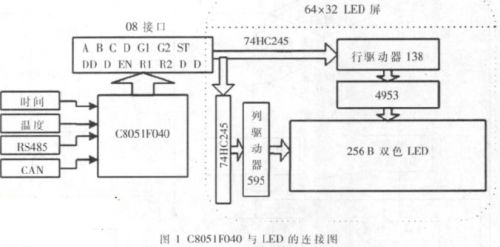
This circuit uses the P3 port of the C8051F040 and the high 3-position control LED of the P3 port. Display, wherein the upper 4 bits of the P2 port are connected to the four address signal lines (ABCD) of the 138 decoder, which are P2.7 connected to A, P2.6 connected to B, P2.5 connected to C, and P2.4 connected to D, P2.3 is connected to G1, P2.2 is connected to G2, P2.1 is connected to CK, P2.0 is connected to ST, P3.7 is connected to EN, and P3.6 is connected to R1 and P3.5 to R2. The clock display circuit uses PCF8563P chip, adopts I2C bus control mode, and SDA and SCL are connected to P1.3 and P1.2 respectively. The temperature circuit adopts 18B20 chip, adopts single bus control mode, and SDA connects to P0.3.
5 C8051F040 control LED Software introduction
(1) Function introduction
This mainly introduces the C8051F040 control LED The split screen displays the date, time, and temperature. According to the hardware connection shown in Figure 1, the row scan software address can be assigned as 0x00, 0x80, 0x40, 0xc0, 0x20, 0xa0, 0x60, 0xe0, 0x10, 0x20, 0x90, 0x50, 0xd0, 0x30, 0xb0, 0x70, 0xf0, The line scan will be performed based on the above address when writing the program.
(2) Software flow chart
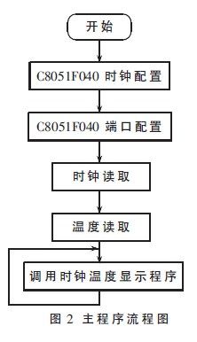
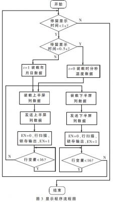
C8051F040 control LED The main program flow chart is shown in Figure 2, and the program flow chart is shown in Figure 3.
(3) C8051F040 source program
The source code of the C8051F040 is as follows.
(1) System clock configuration
Void SYSCLK_Init (void)
{ int i = 0;
SFRPAGE = CONFIG_PAGE;
OSCXCN = 0x67;
For (i = 0; i < 3000; i++);
// Wait 1ms for initialization
While ((OSCXCN & 0x80) == 0);
CLKSEL = 0x01;
OSCICN = 0x00; }
(2) System port configuration
Void PORT_Init()
{ SFRPAGE = CONFIG_PAGE;
//st SFR page before writing to XBR0 = 0x04
/ / Allow UART0, RX, TX to connect to 2 port pins XBR0 = 00000100 P1MDOUT = 0xf0; / / push-pull output
P2MDOUT = 0xff;
P3MDOUT=0xff;
P4MDOUT=0x00; //drain open drain output
P4 |= 0xff; //Write 1 disable low-end output driver
P0MDOUT |= 0x01; //Enable TX0 as push-pull output
XBR2 = 0x42;
}
(4) Connection of PCF8563 and C8051F040
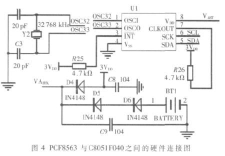
The hardware connection diagram between PCF8563 and C8051F040 is shown in Figure 4.
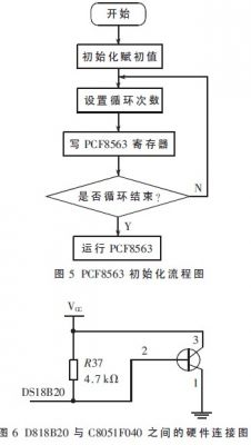
(5) PCF8563 initialization process
The PCF8563 initialization flow chart is shown in Figure 5.
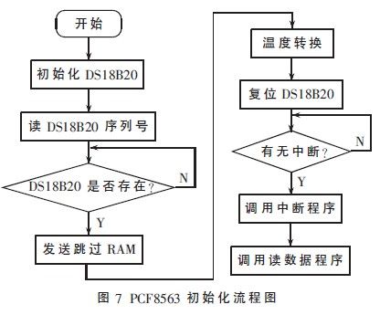
(6) Connection of DS18B20 and C8051F040
The hardware connection diagram between DS18B20 and C8051F040 is shown in Figure 6.
(7) DS18B20 temperature measurement system
Flowchart 7 of the DS18B20 temperature measurement system.
This article mainly introduces LED The working principle of the display, the composition of the hardware circuit, and the requirements for the control system of the single-chip microcomputer, etc., use the unique advantages of C8051F040 to realize the LED Effective control, can directly drive the LED There is no need to add a bus driver to the control board to save system resources. This article also gives the specific part of the software flow chart and source code, which can be displayed normally after the connection according to the hardware connection diagram. This article is in LED The application of the display has certain reference and application value.
Incremental encoders provide speed, direction and relative position feedback by generating a stream of binary pulses proportional to the rotation of a motor or driven shaft. Lander offers both optical and magnetic incremental encoders in 4 mounting options: shafted with coupling, hollow-shaft, hub-shaft or bearingless. Single channel incremental encoders can measure speed which dual channel or quadrature encoders (AB) can interpret direction based on the phase relationship between the 2 channels. Indexed quadrature encoders (ABZ) are also available for homing location are startup.
Incremental Encoder,6Mm Solid Shaft Encoder,Hollow Rotary Encoder,Elevator Door Encoder
Jilin Lander Intelligent Technology Co., Ltd , https://www.jilinlandermotor.com