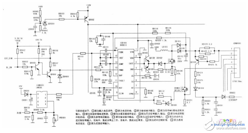
The following figure shows a group of LED backlight driving circuits in Changhong ITV46920DE LED LCD TV. Each group of circuits has the same structure and is independent of each other. Each group of circuits drives an LED lamp group) application circuit. The output voltage of the LED drive circuit is 170V / 90mA. Like the backlight driver circuit in the Hisense LED LCD TV seen earlier, the integrated block HV9911NCJ in the backlight driver circuit is also an LED backlight driver IC. The integrated block has built-in single-switch drive mode controller, high-side current detection circuit, output current closed-loop control circuit, high PWM dimming ratio circuit, 9V ~ 250V internal linear regulator, constant frequency or constant off-time control circuit , VDD = 10V output short circuit protection circuit, output overvoltage protection, synchronous lock circuit, programmable MOSFET current limit circuit, soft start and many other module circuits.
The working process of the LED backlight driving circuit in the following figure is: when the switching power supply is changed from the standby state to the normal working state, the voltage of 130V output by the power supply is divided by the resistors R9006, R9005, R9004, and a voltage of about 2.47V is formed on R9004. Added to the gate of ZDT9001, ZDT9001 is turned on. At this time, the 12V voltage goes to ground through R9011, R9010, and ZDT9001. After the voltage is divided, a voltage of 11.25V is formed on R9010H. This voltage is applied to the base of Q9002 to make Q9002 saturated and conductive. At this time, the 12V voltage passes through the Q9002e-c pole. The output from the C pole to the â‘ pin of the HV9911NG (note: will also be added to the â‘ pin of IC9201, IC9301, IC9401, IC9501, IC9601) as the operating voltage of HV9911NG (IC9201, IC9301, IC9401, IC9501, IC9601).
At the same time, the start control voltage "BL_ON" (high level) of the backlight driver circuit output from the signal processing board is divided by the resistor R9013 and the resistor R9003 to form a 0.56V voltage and applied to the base of Q9003, making Q9003 saturated and conducting . The collector voltage changes from high level to low level. At this time, Q9004 enters the cut-off state because there is no voltage at the base. The + 5VS voltage is added to pin 13 of IC9101 through R9016 and R9017 (note: it will also be added at the same time. To the 13th pin of IC9201, IC9301, IC9401, IC9501, IC9601). After the pins 1 and 13 of IC9101 are powered up, the internal oscillation circuit will start to enter the working state and generate oscillation pulse signals. The oscillating pulse signal generated by the oscillating circuit is processed by the internal related circuit and then output from the â‘¢ pin of the integrated block, which is directly added to the base of Q9102 and Q9103 as its input signal.
The reference voltage (1, 24V) formed by the internal reference voltage generating circuit of HV9911NG is output from pin â‘©. This reference voltage is added to pin HV9911NG (15) via resistor R9107 as the reference voltage of this pin.
HV9911NG⑦ pin external resistor R9105 is a frequency setting resistor. Changing the size of this resistor can adjust the frequency of the oscillator. Once the resistance of resistor R9105 is determined, the oscillation frequency of the oscillator will be determined accordingly. After that, the oscillator will work according to the set natural oscillation frequency.
The drive pulse signal output by the HV9911NG â‘¢ pin is amplified by Q9012, and then added to the gate of Q9101 through resistor R9101 to make Q9101 work in the switching state.
After Q9101 is turned on, the current forms a loop through 130V → L9101 → Q9101 “D†pole → Q9101 “S†pole → R9102 → ground, and stores energy in L9101, generating left positive and negative negative voltages. After Q9101 is cut off, since the current at both ends of the inductor cannot be abruptly changed, a left-negative-right-positive voltage is formed across L9101. This voltage charges capacitor C9110 through D9101 and D9105, causing a voltage of 130V + L901 to charge C9110. The result of this kind of voltage superposition results in a DC voltage of 170V / 90mA, which is added to the LED light-emitting diode (light bar) through resistors R9128 and R9129 as the driving voltage for lighting the LED light bar.
In the circuit, the circuit composed of Q9103 and D9102 is a perfusion circuit. The function of this circuit is the same as the perfusion circuit in the drive circuit of the Hisense LED LCD TV backlight lamp introduced earlier. It is to discharge between the gate and the source of Q9101 during the off period. Designed to store the charge.
The working process of the perfusion circuit is: when the ③ pin of HV9911NG outputs a low level, Q9102 is turned off and Q9103 is turned on. After Q9102 is turned off, the source voltage is low, and Q9101 turns from on to off. At this time, since Q9103 is turned on, the charge accumulated on the gate of Q9101 will be discharged through D9102 → Q9102 source → Q9102 drain, thus effectively avoiding the damage of Q9101 due to the accumulation of charge between the gate and the source.
In order to make the switch tube in the bootstrap booster circuit abnormal, it does not expand the fault range, the circuit also designed a current feedback circuit composed of R9602, R9603 and HV9911NG ⑤ pin internal related circuits. R9602 in the circuit is the sampling resistance, and the foot is the input terminal of the current feedback detection signal. The current feedback circuit is realized by the current detection of the switch tube Q9101. When the switching tube Q9101 works abnormally, resulting in an increase in the current flowing between its drain and source, the voltage drop on the resistor R9102 will increase. The increased voltage is added to the HV9911 ⑤ pin through R9103 and enters the internal circuit of the integrated block. The relevant circuit performs the processing, and outputs the control signal to the drive pulse output circuit after the processing to stop it from working without a pulse signal output, thereby realizing the overcurrent protection of the switch tube.
The Changhong ITV46920DE LED LCD TV backlight driver is designed with a brightness setting circuit, which is composed of R9018, R9019, R9003, VR9001, and ICM9001.
In the figure below, the 12V voltage is divided by a series circuit composed of resistors R9018 and R9019 to obtain a voltage of about 3.58V on R9019. This voltage is then divided by resistor R9003 and potentiometer VR9001 and added to the â‘¢ pin of integrated block ICM9001, â‘¢ The pin is the positive input terminal of the internal comparator.
The â‘ pin of ICM9001 is connected to the 15 pin of HV9911NG through resistor R9002. HV9911NG (15) pin is the current setting terminal of the drive pulse forming circuit. When the potentiometer VR9001 is adjusted to change the â‘¢ pin potential of ICM9001, the â‘ pin voltage Change, â‘ foot voltage change is HV9911NG (15) foot output current setting changes, (15) foot setting current change will inevitably change the width of the output pulse of the driving pulse forming circuit, and finally achieve the purpose of adjusting the backlight brightness according to the design requirements .
The current stabilization circuit in the backlight driving circuit is composed of Q9104, R9121 and the internal related circuit of the integrated block HV9911NG (16) pin.
When the current flowing through the LED light bar increases or decreases, the current flowing through Q9104 and R9121 will also increase or decrease, and the voltage drop formed by the changing current on R9121 will also increase or decrease. The voltage reflecting the current of the LED light bar formed on R9121 is added to the (16) pin of HV9911NG through R9120. After being processed by the internal related circuit of HV9911NG, the control signal is output to control the duty cycle of the integrated block â‘¢ pin drive pulse. The adjustment of the pulse duty ratio returns the LED light bar current to a normal value, thereby realizing the stability of the LED light bar current.
The protection circuit in the backlight lamp driving circuit is divided into overvoltage and overcurrent protection.
The overvoltage protection circuit is mainly composed of R9114, R9115, R9116 and the integrated circuit inside the integrated block HV9911NG (12) pin. When the output voltage of the LED drive circuit is abnormally increased for some reason, the increased voltage is added to the integrated block HV9911NG (12) pin, (12) pin input after being divided by the series circuit composed of R9114, R9115, R9116 After the voltage is processed by a protection circuit such as a voltage comparator inside the integrated block, a control signal is output to the drive pulse output circuit, so that it stops working without a drive pulse output.
The overcurrent protection circuit is realized by stopping the main power supply to work, which is composed of R9128, R9129, R9123, R9124, R9125, Q9105, D9104. The overcurrent protection circuit is aimed at the short-circuit protection of the light-emitting diodes inside the LED light bar.
When the TV is normal, due to the small current flowing through the resistors R9128 and R9129, the voltage drop across it is also low. The base voltage of the Q9105 is basically the same as the emitter voltage. The Q9105 is cut off, which is equivalent to the overcurrent protection circuit stopping working. When the light-emitting diode on the LED light bar inside the screen has a serious breakdown short circuit fault, the LED light bar current will increase sharply. At this time, the base voltage of Q9105 will drop sharply, turning Q9105 from off to on, and the 170V voltage output by the drive circuit is added to the QB857's via the emitter, collector, R9124, R9125, D9104, DB9006, RB883 The base electrode saturates the QB857, the optocoupler PCB803S in the main power supply enters the working state, and the secondary output overcurrent detection signal is sent to the â‘© pin of the integrated block IC801 in the main power supply. After processing, the control signal is output to stop the main power supply in the switching power supply.
ZGAR bar 4000 Puffs
ZGAR electronic cigarette uses high-tech R&D, food grade disposable pod device and high-quality raw material. All package designs are Original IP. Our designer team is from Hong Kong. We have very high requirements for product quality, flavors taste and packaging design. The E-liquid is imported, materials are food grade, and assembly plant is medical-grade dust-free workshops.
Our products include disposable e-cigarettes, rechargeable e-cigarettes, rechargreable disposable vape pen, and various of flavors of cigarette cartridges. From 600puffs to 5000puffs, ZGAR bar Disposable offer high-tech R&D, E-cigarette improves battery capacity, We offer various of flavors and support customization. And printing designs can be customized. We have our own professional team and competitive quotations for any OEM or ODM works.
We supply OEM rechargeable disposable vape pen,OEM disposable electronic cigarette,ODM disposable vape pen,ODM disposable electronic cigarette,OEM/ODM vape pen e-cigarette,OEM/ODM atomizer device.

Disposable Vape, bar 4000puffs, ZGAR bar disposable, Disposable E-cigarette, OEM/ODM disposable vape pen atomizer Device E-cig
ZGAR INTERNATIONAL(HK)CO., LIMITED , https://www.szvape-pods.com