The new low VCEsat BJT technology provides a viable, low-cost alternative to traditional planar MOSFETs (current applications between 500mA and 5A). The low VCEsat BJT helps designers design lower cost, more competitive products.
This article refers to the address: http://
Designers of portable products such as cell phones, digital cameras, digital camcorders, DVD players, MP3 players and personal digital assistants have been under pressure to reduce material costs without affecting product performance, which is for designers. Words are a real challenge because they both add new product features and have a negative impact on battery life.
Most portable products are moving toward integrated power management unit (PMU) circuits designed to control different functions in the product, including battery charging, battery management, overvoltage protection, backlighting, vibrators, disk drives Control of peripherals, powering the camera and flash unit, etc. Circuits that control currents below 500 mA are typically embedded in the PMU, including the final stage regulator. However, if the current is controlled in the range of 500 mA to 5 A, an external transfer tube (MOSFET) is the preferred design. This article compares the MOSFET to the low VCEsat bipolar junction transistor (BJT). It can be seen that the latter can not only reduce power consumption, but also save costs.
The low VCEsat BJT functions the same as the MOSFET, but at a lower cost and, in many cases, consumes less power and therefore has a longer battery life. The lower VCEsat BJT devices use technology developed more than 20 years ago. Today, this technology focuses on reducing the forward saturation voltage to achieve very low forward resistance. At currents of 1A, some new low VCEsat BJTs currently have saturation voltages well below 100mV. This means that the forward resistance is less than 100mΩ, making it competitive with higher cost MOSFETs.
Design considerations
The MOSFET is a voltage driven device and the low VCEsat BJT is a current driven device. Therefore, designers need to understand the current limit of the PMU control circuit used to determine the specific circuit requirements for design with low VCEsat BJT. For example, if the low VCEsat BJT is to control 1A current and its worst case amplification is 100, then the base current must be at least 10mA to ensure that the low VCEsat BJT is saturated. The control pin must be capable of supplying 10mA to the low VCEsat BJT for direct drive, otherwise an additional drive segment is required.
Charging circuit example analysis
As can be seen from the charging circuit of the portable product (see Figures 1, 2), the low VCEsat BJT and a resistor are used instead of the regulating tube Q1 (power MOSFET 2A, 20V, TSOP6 package) and the Schottky diode D1 is blocked. In this example, the low VCEsat BJT saves $0.10 over typical MOSFETs and reduces power consumption by 261 mW.
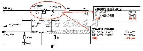
Figure 1 Charging circuit cost and power consumption of MOSFET and Schottky diode
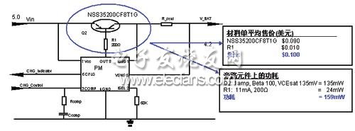
Figure 2 Cost and power consumption of a charging circuit using low VCEsat BJT and bias resistors
Lithium-ion battery charge control devices are embedded in the PMU. The PMU control pin goes high to turn on the external regulator Q1 and the charge current is set to 1A. The Schottky diode D1 connected in series needs to block the reverse current of the battery.
The typical power dissipation on regulator Q1 and reverse blocking diode D1 can be calculated as follows:
Q1 power consumption = I2 × R, I = 1A, RDS (ON) = 60mΩ, Q1 power consumption = 60mW
D1 power consumption = I × VF, I = 1A, VF = 360mV, D1 power consumption = 360mW
Total power consumption on Q1 and D1 = 420mW
The high-volume cost of MOSFETs and Schottky diodes is typically $0.175.
The charging circuit can be configured with a low VCEsat BJT to replace the MOSFET and Schottky diode. Since the low VCEsat BJT design itself has this feature, there is no need for Schottky diodes. The control pin on the PMU provides a maximum current of 20mA. The PMU can initiate a fast charge with a battery voltage of 3.0V. When Q2 is saturated, the collector and emitter voltages are approximately 3.0V, so the base voltage is 2.3V. At a charge current of 1A, the base current required to drive the ON Semiconductor NSS35200CF8T1G low VCEsat BJT (minimum gain of 100) to the saturation region should be 10mA. Selecting a standard resistance of 200Ω for the base resistor ensures that the low VCEsat BJT is in the saturation region and does not exceed the drive pin limit.
The typical power dissipation on regulator Q2 and bias resistor R1 can be calculated as follows:
Q2 power consumption = I × V, I =1A, VCEsat = 135mV, Q2 power consumption = 135mW
R1 power consumption = I2 × R, I = 1A, R = 200Ω, R1 power consumption = 24mW
Total power consumption on Q2 and R1 = 159mW
The high cost of low VCEsat BJT and resistors is typically $0.10.
As can be seen from the above calculations, replacing the MOSFET regulator and Schottky diode with a low VCEsat BJT and bias resistor can save $0.075 per device, while also reducing power consumption by 261mW, making the thermal design of portable products It's even simpler.
More complicated circuit
An integrated circuit specifically designed with a MOSFET pass transistor may not provide the required current to drive the low VCEsat BJT directly into the saturation region. Among these circuits, an additional digital transistor or a small general-purpose MOSFET (Q4) can be used as shown in FIG.
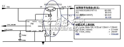
Figure 3 Charging circuit cost and power consumption of additional digital transistors or small general-purpose MOSFETs
The results are not very obvious compared to the charging example. The cost savings are still $0.055 per device, with the same power consumption.
More advantages with low VCEsat BJT
BJT is not susceptible to ESD damage and therefore does not provide additional ESD protection, which can save costs. Since the turn-on voltage of the BJT is low (typical: 0.7V), the oscillator and charge pump circuits normally required for MOSFETs can be eliminated. BJT is more efficient at converting medium currents.
ZGAR Vape Device 5.0
ZGAR electronic cigarette uses high-tech R&D, food grade disposable pod device and high-quality raw material. All package designs are Original IP. Our designer team is from Hong Kong. We have very high requirements for product quality, flavors taste and packaging design. The E-liquid is imported, materials are food grade, and assembly plant is medical-grade dust-free workshops.
From production to packaging, the whole system of tracking, efficient and orderly process, achieving daily efficient output. We pay attention to the details of each process control. The first class dust-free production workshop has passed the GMP food and drug production standard certification, ensuring quality and safety. We choose the products with a traceability system, which can not only effectively track and trace all kinds of data, but also ensure good product quality.
We offer best price, high quality Vape Device, E-Cigarette Vape Pen, Disposable Device Vape,Vape Pen Atomizer, Electronic cigarette to all over the world.
Much Better Vaping Experience!


ZGAR 5.0 E-Cigarette Vape Pen,ZGAR 5.0 Device Vape,ZGAR Vape Device 5.0 Vape Pen Atomizer,ZGAR Vape Device 5.0 Disposable E-Cigarette OEM vape pen,ZGAR Device 5.0 electronic cigarette
Zgar International (M) SDN BHD , https://www.zgarpods.com