In embedded systems, in addition to embedded processors, programmable logic devices are often used. Some programmable logic devices can also update their programs after being soldered to a printed circuit board. This feature is called "In System Reprogrammability (ISR)". During board development, the programmable logic device is typically reprogrammed through the IEEE Standard 1149.1 JTAG interface using a download cable. During the product prototype and manufacturing stage, the JTAG interface on the board is likely to be unable to connect with the download cable due to product outline and internal structure design. In this case, the programmable logic device cannot be reprogrammed through the download cable. Products based on embedded systems are usually externally provided with serial or Ethernet interfaces. These interfaces are controlled by embedded processors [1]. Therefore, these interfaces can be used to send programmable logic device update programs to processors. The device reprograms the programmable logic device.
2 implementation methods2.1 Software aspects
The serial interface is widely used by the embedded system because of the simple protocol implementation and low resource consumption. Only the serial interface cable is used to connect the serial interface of the host with the serial interface of the product, and the serial interface is communicated via the host computer. The software sends the update program to the processor. The file transfer protocol generally uses the Xmodem protocol. For an embedded system-based network product, the Ethernet interface is provided by itself, and the operating system has a built-in TCP/IP protocol stack. You can use the Ethernet interface to send updates to the processor. The file transfer protocol typically uses the TFTP protocol, the embedded system runs the TFTP server program, and the host runs the TFTP client program [2].
The updater of the programmable logic device received by the embedded processor through the serial interface or the Ethernet interface is a Jam file using a development tool similar to the Quartus II development tool of Altera Corporation according to the Jam standard and test language (Jam Standard Test). AndProgramming Language (hereinafter referred to as the Jam language) requires the conversion of a target file such as Programmer Object File (*.pof, file name pof) [3]. The Jam file is an ASCII file that contains all the information needed to program a programmable logic device, including programming algorithms and data, as described in detail below:
(1) The "Note field" section stores information about the Jam file, including the name of the programmable logic device, the creation time of the Jam file, the version of the Jam language used, and so on.
(2) The "Variable declaration/initialization" section consists of program/verification data and some variable declarations used by the Jam file.
(3) The "algorithm part" contains the commands and codes needed to program the programmable logic device, including blank check, erase, program, and check, etc. All functions that can be performed on the programmable logic device. Branch or loop structures can be used in the code.
The embedded processor parses the Jam file by running a Jam Player program after receiving the Jam file, translates each instruction in the file, and performs data read and write operations on the JTAG port, thereby completing the program for the ISR programmable logic device. Update work. Jam Player is a C language program whose main main program performs all basic functions, including parsing of Jam file contents, instruction translation, etc. This part is the same for all embedded systems and Jam files. The Jam Player's I/O functions, including I/O pin addressing, time-delay programs, file I/O, and operating system-related functions are all contained in the jamstub.c file. By modifying this file Jam Player can Suitable for any system structure. When the Jam Player receives data, jamstub.c can retrieve data from the Jam file or read data from the TDO pin. Jamstub.c can also send processed JTAG data to three JTAG pins (TDI, TMS, and TCK), returning error messages and related information to the calling program. Programs that upgrade ISR programmable logic devices only need to change the Jam file.
The Jam Player controls read and write operations on the JTAG interface through a jam_jtag_io function (int jam_jtag_io(int tms_tdi)). Each time this function is called, the JTAG's TMS and TDI output signals will be set to the desired values, and the TDO input signal will be sampled and the value will be returned, after which the TCK clock signal will generate a falling edge. The tms_tdi parameter contains 3-bit information indicating the status of the TMS signal and the TDI signal, respectively, and whether or not the TDO output needs to be read (the TDO read operation can be skipped if no TDO value is used). The lowest bit represents the value of TMS, the second bit represents the value of TDI, and the third bit indicates whether to read TDO: if set, the value of TDO must be read, otherwise it is not needed. If TDO is low, zero is returned and high returns a non-zero value. If TDO is not read, it will return zero.
2.2 Hardware aspects
There are two ways to connect an embedded processor to a JTAG device. One is to connect the embedded processor directly to the JTAG device. This method requires a dedicated four pins for the JTAG interface, saving board space. While the space occupies the four pins of the processor, the other method uses an interface logic to connect the JTAG device to the bus of the processor. The processor reads and writes the JTAG device through the corresponding address [4] .
Figure 1 shows an example of interface logic. When the interface logic receives the correct address and control signals, it will synchronize the TDI, TCK and TMS signals and drive the output pins through the multiplexer. The download cable can also be used to perform JTAG chaining through the multiplexer. Programming or verification [5]. Synchronization of TDI, TCK, and TMS signals is accomplished through the embedded processor's clock signals and registers. The TDO's buffer prevents bus contention. The TDI, TCK, and TMS buffers can also be used to read back registers during debugging. value. The AND gates in the figure control read or write operations through R/W signals, while the AS and DS signals can select and deselect circuits at another level.
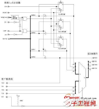
â–² Figure 1 Interface Logic
2.3 Memory Usage
The following discusses the use of memory when reprogramming a programmable logic device using an embedded processor. In order to be compatible with embedded processors that do not have memory allocation services, Jam Player requires not only program memory space but also dynamic memory. Program memory (such as a hard drive or ROM) is used to store Jam Player executable binaries and Jam files; dynamic memory (such as RAM) will be used when the Jam Player is called.
Jam Player Follow these steps to use memory:
(1) The embedded processor calls Jam Player from ROM;
(2) Jam Player reads the Jam file from the ROM and then stores it in RAM;
(3) Jam Player decompresses the compressed program data contained in the Jam file, and stores the decompressed data in RAM;
(4) The Jam Player initializes a symbol table, a stack, and a heap in RAM.
The symbol table contains the labels and variables of the Jam file; the stack is used for FOR loops, CALL and PUSH statements; the heap acts as a temporary memory for evaluation of mathematical expressions and storage of padding data. Each command stack and heap size encountered while processing the Jam file will increase, the available dynamic memory will be less and less, and the Jam file, the decompressed data, and the dynamic memory space required by the symbol table will not remain in the process. change.
The Jam Player memory usage is shown in Figure 2.
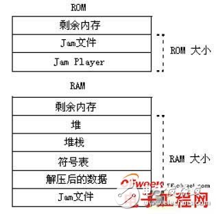
â–² Figure 2 Jam Player memory usage
2.3.1 Program Memory Space (ROM) Usage
The required program storage space is:

The size of the Jam Player is determined by the complexity of the embedded processor used and the interface logic. The total program memory space of the Jam file is determined by the number of devices being programmed on the JTAG chain. If there is only one device in the JTAG chain, the size of the corresponding Jam file for that device is the size of the required program memory space. The size of the Jam file also depends on the target device, typically between 26K bytes and 30K bytes after compression. Assuming there are 3 devices in the JTAG chain, all 3 devices will be programmed and the required Jam file storage space will be the sum of the 3 Jam file sizes. Table 1 shows the program memory space required for a single device.
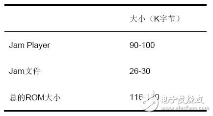
â–² Table 1 The program memory space required by a single device
2.3.2 Dynamic Memory (RAM) Usage
The required RAM space is:

Jam files require the same amount of RAM space as ROM space and have been discussed in the context of program memory space usage. After the Jam Player reads the Jam file from the ROM and stores it in RAM, the Jam Player decompresses the compressed data in the Jam file and stores the decompressed data in RAM. The size of the decompressed data in RAM can be obtained from the ACA variable in the Jam file. Each ACA variable is listed in the Variable Declaration/Initialization section. The size of each array is determined by the value in the variable declaration square brackets. E.g:

The decompressed ACA variable size is 434460 bits, which is approximately 53K bytes.
The size of the symbol table is given by:

The size of a variable or tag name is 48 bytes, and JAM_C_MAX_SYMBOL_COUNT is defined in the jamdefs.h file. The default value is 1021. In fact most Jam files use up to 400 variables and tag names. Modifying JAM_C_MAX_SYMBOL_COUNT to 400 saves some dynamic memory,

Compared to the total RAM space used by the Jam Player, the stack and heap require very little RAM, and the JAMC_MAX_NESTING_DEPTH constant in the jamdefs.h file defines the maximum depth of the stack. Table 2 shows the required RAM space for a single device.
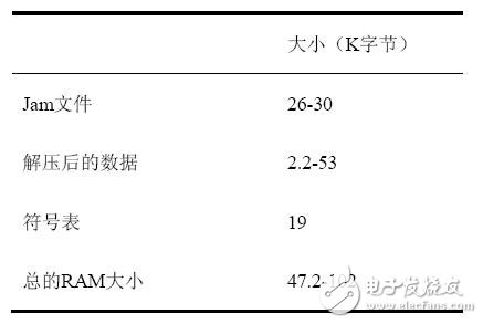
â–² Table 2 RAM Space Required for a Single Device
3 ConclusionThis article describes in detail the use of software, hardware, and memory usage, and describes in detail a new method for reprogramming ISR devices using the Jam programming and test language through an embedded processor, which is programmable during product prototype and manufacturing stages. Logical device reprogramming provides a reference and has a strong practical significance.
The author of this article innovates: Since the JTAG interface on the board is likely to be unable to connect with the download cable due to product form and internal structure design considerations during the product prototype and manufacturing stage, it will not be possible to download the cable to the programmable logic. Device reprogramming. Sending the update program of the programmable logic device to the processor via the serial interface or the Ethernet interface reprograms the programmable logic device by the processor, solving this problem.
For example, GEEKVAPE Z Series Coil. The Geekvape Z(zeus) Sub-Ohm Mesh Replacement Coils are a set of kanthal meshed heating element coil atomizers built for the new Geekvape Z(zeus) Sub-Ohm Tank, the latest variant in the tried-and-true Z lineage. The mesh coils are installed in a plug 'n' play fashion from the bottom threaded tank base. It comes in a pack of five.
Applicable Models
Geekvape L200(Aegis legend 2) kit
Geekvape Z(Zeus) sub ohm tank 2021
Geekvape Z(Zeus) sub ohm tank
Geekvape Obelisk tank
Geekvape Obelisk 120FC Z Kit
Geekvape Aegis X Zeus Kit 200W (Z Edition Only)
Geekvape P Sub Ohm Tank
geekvape vape coils and pods,geekvape vape coil wire,geekvape vape coils kit,geekvape vape coils mesh,geekvape vape coils mod
Ningbo Autrends International Trade Co.,Ltd. , https://www.ecigarettevapepods.com