The integrated circuit (IC) design team is often under tremendous pressure as the scheduled tape delivery deadline approaches. To make matters worse, they often face a later engineering change order (Engineering Change Order), which can lead to extra time-consuming work, such as the need to completely re-layout the layout due to a small change. For 45 nm and below, the new manufacturing requirements not only greatly increase the complexity of the metal fill location, but also significantly increase the number of fill components in the design. The purpose of the filling has changed, previously to ensure the lowest metal density in the entire layout, but now to achieve the maximum target density. In addition, the density gradient check was developed to ensure a smooth transition between the packing densities in adjacent locations. For 20 nm and below, the fill requirements must also include multiple exposure limits to ensure mask balance, and the design engineer not only needs to add multiple layers of fill on the back end of the process (BEOL) metal and vias and The layers in the front-end process (FEOL) also need to be added.
All of these changes regarding padding require support for complex new fill types and fill strategies, as padding no longer only affects flatness issues and has been extended to multiple manufacturability issues. Filling now also directly affects the performance of the design. Technologies such as cell-based fill and multiple exposure-aware fill have been developed and integrated into the fill engine, providing the design team with an auto-fill process that can be called directly from the Auto Place and Route (P&R) tool to ensure its convenience. Develop the design process and get the right design results. However, in order to get an accurate and optimized fill position, designers need a specially adapted environment to cope with the ever-increasing new inspection and restriction requirements.
Wiring tools are used to create millions of connections that do not meet complex cross-layer fill requirements. The number of filled graphics in new technologies is likely to exceed one billion new objects, making the challenges of P&R systems even more complicated. ECOs that are late in the manufacturing process must be processed efficiently and accurately, otherwise the complexity of replacing fillers and reconfirming timing can adversely affect file size, run time, and timing closure, leading to delivery of manufacturing deliveries. delay. To balance timing analysis in P&R system uptime, the EDA industry has developed a process in which all filled graphics are stored in a separate file on disk, using an extraction tool to combine them with the layout file. This process does not slow down the back-end process when calculating the impact of timing.
In order to solve these problems, an effective ECO fill strategy must be accurate and fast, while only focusing on the design part affected by the ECO. By removing and replacing padding in the region and re-validating the timing within the affected region, we can reduce run time, manage file size, and minimize the impact of timing (Figure 1). By strictly limiting the ECO fill operation only where the actual reticle fabrication changes, we can limit the size of the area where the error must be evaluated, edited, and refilled. This area reduction method first generates an exclusion zone and then clips the fillable database to the area surrounding only the design ECO. If designers can use the same Design Rule Check (DRC) sign-off tool as foundry, it will be easier to reduce these areas more accurately.
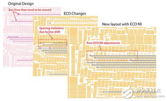
Figure 1. The fill ECO policy adjusts the padding around the ECO changes, eliminating the need to regenerate the entire layout for the entire layout, saving valuable time for delivery deadlines.
Another issue is the size of the database. Simply deleting the fill pattern around the ECO area requires flattening the fill hierarchy, which can cause the fill database to explode. To solve this problem, the intelligent ECO fill technique first finds the cells that contain the fillers that need to be deleted that conflict with the ECO design graphics, and then flattens the minimum number of cells at the lowest level in the fill hierarchy. It then repopulates only the area where the ECO change occurred, rather than refilling the entire chip.
By strictly limiting the ECO fill operation only where the actual mask production changes, we can limit the size of the area where the error must be evaluated, edited, and refilled. This area reduction method first generates an exclusion zone and then clips the fillable database to the area surrounding only the design ECO. Obviously, there is a balance here. If the area to be refilled is too large, this strategy cannot guarantee scale and precision. In general, ECO fill strategies are most effective when changing design areas that affect less than 1%. This is not the case, in fact, the ECO fill process may run longer than the normal fill process. However, in this case, the designer must also consider whether the effects of timing and the cost of the mask can be minimized to offset the runtime disadvantage.
Multiple small change regions are more suitable for selecting ECO fill strategies, such as changes in gate functions that require local path rewinding within a limited area. To change the entire block more efficiently, just refill the design from scratch, and in these cases, tiering is a good choice.
To take advantage of these new fill technologies, not only does the tool need to provide the required functionality, but it is also critical that the foundry provide supporting documentation that makes the process easy to use. As designers become more aware of ECO fill technology, they will be able to use these technologies in their design processes to better manage post-design changes and maintain the delivery schedule for advanced process designs.
Ceramic Insulator,Ceramic Electrical Insulators,Ceramic Standoff Insulators,Ceramic Isolators
Yixing Guangming Special Ceramics Co.,Ltd , https://www.yxgmtc.com