The responder generally has multiple answering inputs and a resetting end. When a certain answering input has a signal input, the answering of this way is successful. The instant after the successful answering can block each of the answering input terminals, so that the following responder signal can not enter the responder, until the reset control signal is valid, the blockade can be released, and the next answer can be made.
There are many types of responder circuits. This design is a circuit with very clear circuit structure functions. Only basic unit circuits such as AND gates, OR gates, and basic RS flip-flops are used in the circuit.
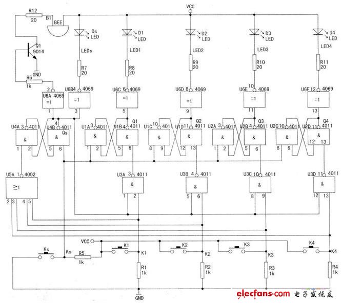
First, the circuit structure and working principle
As shown in the figure below, the whole circuit can be divided into signal input control circuit, effective signal storage circuit, output drive and indication circuit.
U3A~U3D4 NAND gates are the rush signal input control gates. Only when U4B outputs a high level, that is, G=1, the rush signal can pass these control gates.
The effective signal storage circuit is realized by four basic RS flip-flops composed of eight NAND gates of UIA to UIB. Before the call is answered, the host needs to press the reset button Ks, and the four basic RS flip-flops are reset. The output of Q1~Q4 is zero. At the same time, when the reset button Ks is pressed, the basic RS flip-flop composed of U4A and U4B is set to 1, that is, U4B outputs a high level, Qs=l, and the four control gates U3A to U3D are opened. If no player presses the answer button, ie, K1~K4 are not closed, due to the action of R1~R44 pull-down resistors, the control gates U3A~U3D are all "see 0 out of 1", output high level. 4 for storage The basic RS flip-flop of the rush signal is in the hold state. Q1~Q4 still output zero; U4B outputs a high level to make the inverter U6B output low level, so that DS emits light, so that it is ready to be answered.
When a certain player presses any of the buttons K1~K4, the rushing signal passes through the control gate, so that the corresponding basic RS flip-flop is set to 1. The corresponding inverter outputs a low level, and the LED of the road emits light. In order to show the success of the answer. For example, when the player presses K2, UID outputs a high level, Q2=1, U6D outputs a low level. D2 illuminates, indicating that player 2 has successfully rushed. At the same time, this rushback causes the NAND gate U5A to output a low level and the basic RS flip-flop composed of U3C and U3D to be flipped so that Qs=0. As a result, the four control gates are blocked, and Kl to K4 are temporarily inoperative, so that the entire circuit is kept in the state where the first button is successfully answered, and the buzzer sounds to indicate that someone has successfully answered. If you need to resume waiting for the answer state, the host clicks the reset button Ks, and the responder resets, and the answer can be answered again.
U6A~U6F are inverting drivers for driving LEDs; Q1 is used to drive buzzer B1; R6 to R11 and R12 are current limiting resistors.
Second, the installation and debugging circuit
Can be installed on the universal circuit board, it is best not to use the breadboard to plug. When choosing a large universal board, it is necessary to pay attention to neatness and wiring when placing components. It is best to wire on the front side and weld on the reverse side.
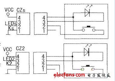
In order to improve the success rate of circuit fabrication, the circuit can be made into a printed circuit board. When designing the printed circuit board, pay attention to the proper distance between the components. If the position of the external button and the indicator socket can be reserved during design, this circuit is a practical responder that can be used in the intelligence test. . The upper right picture shows the connection diagram of the external circuit of the host, and the lower right picture shows the connection diagram of the external circuit of the player 2.
The NAND gate in the circuit uses a CMOS integrated circuit 4011 with four NAND gates inside, or a non-gate 4002. The drive circuit uses a 4069 with an inverting function. The buzzer is rated at 3V. DC buzzer. The debugging of this circuit is extremely simple, and the welding is good. After the inspection is correct, the correct power supply voltage can be added to realize the answering function. Since the circuit uses a 4000 series CMOS integrated circuit, the voltage of the circuit is widely used (3~18V). However, it is generally better to add a voltage of about 5V. Please select the parameters of the LED and the buzzer current limiting resistor for debugging. The brightness of the LED and the loudness of the buzzer are moderate. Generally, the current of the LED should be 5 mA to 10 mA, and the current of the buzzer should be 20 mA to 30 mA.
Ring Type Connecting Terminals
Taixing Longyi Terminals Co.,Ltd. , https://www.lycopperterminals.com