The MAC57D5xx family is targeted at next-generation device platforms that use the single and dual high-resolution display instrument cluster market. Utilizing the highly successful MPC56xxS product family, NXP has introduced a multi-core architecture using ARM Cortex-M (real-time) and Cortex-A processors (for applications and HMI), integrating 2D graphics accelerator (GPU) and head-up display (HUD) Curved engine, dual TFT display driver, stepper motor drive and powerful I/O processor provide cost-effective cutting edge performance and scalability.
Powered by ARMR CortexR-M and Cortex-A processors, these products integrate 2D graphics accelerators, head-up display surface engines, dual TFT display drivers, integrated stepper motor controllers and powerful I/O processors. Provides cost-effective cutting edge performance and scalability.
The series supports up to two WVGA resolution displays, including a display with a line-up display (HUD) surface engine. Generating graphical content with powerful Viviane GPUs and 2D animation and compositing engines (2D-ACE) that support OpenVG 1.1 greatly reduces the memory footprint of content creation. Embedded memory includes up to 4MB of flash, 1MB of SRAM with ECC and up to 1.3MB of graphics SRAM without ECC. Memory expansion is available through the DDR2 and SDR DRAM interfaces, while two flexible QuadSPI modules provide SDR and DDR serial flash expansion. In response to growing security and security requirements, the MAC57D5/4xx family integrates NXP's latest, SHE-compliant CSE2 engine and supports ISO26262 ASIL-B functional safety compliance.
Main features of MAC57D5xx
ARM Cortex-A5, 32-bit CPU
Support ARMv7-ISA
32KB instruction cache, 32KB data cache
NEON SIMD media processing engine
FPU supports double precision floating point arithmetic
Memory management unit
GIC interrupt controller
Up to 320MHz
ARM Cortex-M4, 32-bit CPU
Support ARMv7-ISA
16KB instruction cache, 16KB data cache
64KB Tightly Coupled Memory (TCM)
Single precision FPU
NVIC interrupt controller
Integer performance per MHz is 1.25 DMIPS
Up to 160MHz
I/O processor
ARM Cortex-M0+, 32-bit CPU
Intelligent stepper motor drive
Memory subsystem
System memory protection unit
Flash controller supports 4MB on-chip flash memory
1MB on-chip SRAM with ECC
1.3MB on-chip graphics SRAM and FlexECC
Support wake-up from low power mode through WKPU controller
On-chip voltage regulator
External 3.3V input power supply
Option to directly supply core voltage externally
Low voltage detection (LVD) and high voltage
Detect on various power supplies and voltage regulators (HVD)
Debugging function
Visibility of the kernel's runtime debug control and system resources using the debug access port (DAP)
IEEE1149.1/IEEE1149.7 System JTAG Controller (SJTAG)
Program and data tracking support (16-bit data width) trace capture by the ARM Trace Port Interface Unit (TPIU)
Timer
Four 8-channel FlexTImer modules (FTM)
Two 4-channel system timer modules (STM)
Three software watchdog timers (SWT)
An 8-channel periodic interrupt timer (PIT)
Automatic real-time counter (RTC)
simulation
1&TImes; 24-channel, 12-bit analog-to-digital converter (ADC)
2 analog comparators (CMP)
Safety
Cryptographic Service Engine (CSE)
ISO26262 ASIL-B Compliance
Support PASS
A fault collection and control unit (FCCU) for collecting faults and issuing interrupts
Multiple operating modes
Includes enhanced low power operation
Memory interface
2 dual QuadSPI serial flash controllers
Support for SDR and DDR serial flash
Support 3.3V Hyperflash (Spansion)
DRAM controller supporting SDR and DDR2
Clock interface
8MHz~40MHz external crystal oscillator (FXOSC)
16MHz IRC (FIRC)
128kHz IRC (SIRC)
32kHz external crystal oscillator (SXOSC)
Clock monitor unit (CMU)
FM phase-locked loop (FMPLL)
Real time counter (RTC)
Graphical interface
Vivante GC355 GPU supports OpenVG1.1
2&TImes; 2D-ACE display controller (with inline top view display surface)
Digital RGB, TCON_0 (RSDS), TCON_1, and OpenLDI/LVDS output options
Digital Video Input (VIU4)
RLE decoder for memory memory decompression
40&TImes; 4-segment LCD driver, reconfigurable to 38×6 or 36×8
Cluster peripheral
Sound Generator Module (SGM)
6 stepper motor driver and step stall detection
Communication
Ethernet 10/100+AVB (ENET)
MLB50
FlexCAN×3
DSPI×5
LINFlexD×3 (1×master/slave, only 2×master)
I2C×2
An eDMA controller with multiple transfer request sources using DMAMUX
Boot Assist Flash (BAF) supports internal flash programming
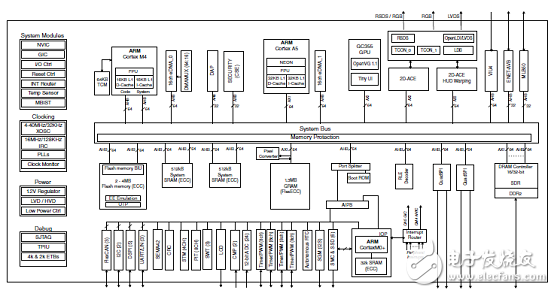
Figure 1 MAC57D5xx high-level block diagram
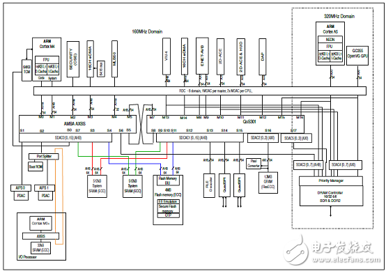
Figure 2 Detailed block diagram of MAC57D5xx
MAC57D5xx Evaluation Board MAC57D5MB
The EVB is designed to provide customers with a low-cost mechanism for evaluating the MAC57D5xx family of microcontrollers and to facilitate hardware and software development. The EVB is suitable for use in bench/laboratory applications and is designed using components specified by ambient temperature. There are two daughter cards that can be connected to the EVB via a high-density connector. For more information, please consult your NXP representative.
Main features of MAC57D5xx evaluation board MAC57D5MB
Main power switch and regulator status LED.
High speed CAN transceiver
LIN interface
Ethernet PHY and RJ45 sockets can be configured as RMII or MII
20-pin JTAG
ARM Cortex connector
ART ETM connector
User reset switch with reset status LED.
User LED
User button switch
A potentiometer connected to the analog input channel.
VIU interface
TFT Display Interface for EastRising Backlight Power Supply - ER-TFT050-3
2 stepper motor connectors
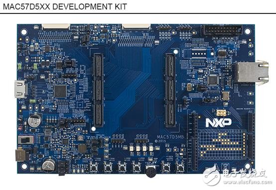
Figure 3 Evaluation board MAC57D5MB outline drawing
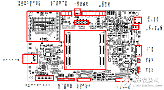
Figure 4 Evaluation board MAC57D5MB component distribution map
a thing that joins together two parts of sth, two vehicles or two pieces of equipment.

Custom Coupling,Coupling Of Encoders,Useful Coupling,Latest Coupling
Yuheng Optics Co., Ltd.(Changchun) , https://www.yhenoptics.com