1) What is the function and principle of adding a ground Via hole near the Via hole of the wire?
The vias of the pcb board are classified according to their functions and can be divided into the following types:
1, signal vias (via structure requirements have minimal impact on the signal)
2, power supply, ground via (via structure requires the smallest distribution of vias)
3, heat dissipation vias (via structure requires minimum thermal resistance of vias)
The via mentioned above belongs to the ground type via, and the grounding Via hole near the Via hole of the trace serves to provide a short return path for the signal. Note: The signal is in the via of the layer, which is a discontinuity of impedance. The return path of the signal will be disconnected from this. In order to reduce the area enclosed by the return path of the signal, some ground must be placed around the signal via. The vias provide the shortest signal return path and reduce the EMI emissions of the signal. This radiation is significantly increased with the increase in signal frequency. 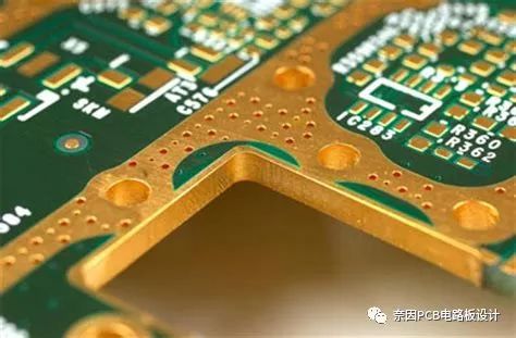
2). Under what circumstances should I use more holes? There is a saying: more holes in the ground will destroy the continuity and integrity of the formation. The effect is counterproductive
First of all, if more holes are made, resulting in the continuity and integrity of the power layer and the ground layer, this situation is resolutely avoided. These vias will affect the integrity of the power supply, resulting in signal integrity issues that are very damaging. Playing the hole, usually occurs in the following three situations:
1. The ground hole is used for heat dissipation;
2. The ground hole is used to connect the stratum of the multi-layer board;
3. The position of the via hole for the high-level signal to be replaced by the ground hole;
3). But all of these situations should be carried out with guaranteed power integrity. That is to say, as long as the spacing of the holes is controlled, is it possible to use more holes? Is there a problem with the ground hole at one-fifth of the wavelength?
If I want to ensure the connection of the ground of the multi-layer board, and more holes, although there is no partition, will it affect the integrity of the formation and power layer?
If the copper layer of the power layer and the ground layer is not affected by the partition, it is not big. In current electronic products, the general EMI test range is up to 1Ghz. Then the 1Ghz signal has a wavelength of 30cm, and the 1Ghz signal has a 1/4 wavelength of 7.5cm = 2952mil. That is to say, if the spacing of the vias can be less than 2952 mils, the connection of the formation can be well satisfied and a good shielding effect can be achieved. Generally we recommend that every 1000 mils to pass through the hole is enough.
gree , https://www.greegroups.com