First of all, when the flyback power supply is generally designed with a duty cycle, we are generally less than 0.5. Everyone knows that if it exceeds 0.5, slope compensation must be added.
So why is the duty cycle of the Switching Power Supply designed to be about 0.45 instead of smaller when designing the flyback switching power supply?
What I hear most is that the larger the duty cycle, the higher the efficiency of the power supply, so everyone designs it this way. In fact, it is also a trend. Why? How to explain it in principle? How do you see from the formula?
Let's analyze it together:
Take the flyback DCM mode as an example
First of all, the three key components that affect the efficiency of the switching power supply are
1. MOS tube
2. Transformer
3. Output rectifier diode
Of course there are other components, but these three account for a relatively large proportion.
MOS tube loss is divided into: turn-on loss, turn-off loss, conduction loss, drive loss
(The turn-on loss in the DCM state is negligible)
Transformer loss is divided into: iron loss, copper loss
Rectifier diode loss is divided into: conduction loss, reverse recovery loss
The parameter most related to these losses is the current: peak current, effective value current.
If we can prove that the larger the duty cycle, the smaller the peak current and the smaller the effective value current, then we can basically confirm our title: the larger the flyback duty cycle, the higher the efficiency.
First put out the formula:
1. Available according to the conservation of energy

Among them, Lp is the inductance of the primary winding, Ip is the peak current of the primary winding, P is the power of the power supply, and T is the duty cycle of the switching power supply.
2. The relationship between current, inductance, voltage and time
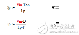
Among them, Vin is the input voltage, Ton is the on-time of the switch in one cycle, D is the duty cycle, Lp is the primary winding inductance, f is the switching frequency, and Ip is the peak current.
3. Substitute Eq. 3 into Eq. 1 to get

Let's look at the following equation four, where the input voltage Vin is fixed, the switching frequency f is also fixed, and the switching power supply power P is also constant.
Therefore, it is easy to see that the larger the duty cycle D is, the larger the calculated primary inductance is. On the contrary, the smaller D is, the smaller the calculated primary inductance is. We call this conclusion the first conclusion.
4. Let's go back and transform formula one to get formula five
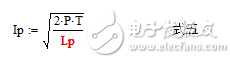
It can be seen from Formula 5 that the larger the Lp, the smaller the peak current Ip, and vice versa, the smaller the Lp, the larger the peak current. In combination with conclusion 1, we can see that the greater the duty cycle D, the smaller the peak current Ip, and the smaller the duty cycle D, the greater the peak current Ip. We call this conclusion the second conclusion.
Let's look at the effective value current under the flyback DCM
1. The effective value current formula of flyback DCM is:

Among them, Iprms is the primary inductor RMS current, Ip is the primary inductor peak current, and D is the duty cycle.
Why is the effective value current this formula?
Since the peak current IP and the duty cycle D are inversely proportional, the relationship between the effective value current Iprms and the duty cycle D cannot be obtained from formula 6 alone. We need to eliminate Ip according to other formulas to prove it.
We can substitute formula 3 and formula 4 into formula 6 to get

Let’s look at formula 7, P is fixed and Vin is fixed, so we can draw a conclusion 3: The larger the duty cycle, the smaller the effective value current, and vice versa, the smaller the duty cycle, the greater the effective value current.
to sum up:
When designing DCM flyback, we pass conclusion two and conclusion three
The larger the duty cycle design, the smaller the peak current and the smaller the effective value current.
The smaller the duty cycle design, the larger the peak current and the larger the effective value current.
Therefore, when designing a flyback power supply, we generally design the maximum duty cycle to be close to 0.5. For example, around 0.45, the efficiency will be higher.
Any QI enabled device like iPhone X/ 8/8Plus, Galaxy, Samsung S7,S7 Edge, S6,S6 Edge, Nexus 4/5/6 (NOTE: Other device have no wireless charging function except putting on extra receivers.)
Starts the moment you place down any Qi-enabled device or device equipped with a Qi-compatible cover. No cables or USB interface required. Input: AT LEAST 5V/2A; Output: 5V/1A
Wireless Charger,Universal Wireless Charger,Portable Wireless Charger,Mobile Wireless Charger
Shenzhen Waweis Technology Co., Ltd. , https://www.laptopsasdapter.com