In recent years, with the rapid development of wireless communication services, the communication frequency band has become increasingly crowded. In 1985, the Federal Communications Commission (FCC) authorized ordinary users to use the three "Industrial, Scientific, and Medical" (ISM) bands of 902 MHz, 2.4 GHz, and 5.8 GHz. The ISM band provides wireless communication equipment with a product frequency band that can be directly used without applying for low transmission power, which greatly promotes the development of the wireless communication industry. Although wireless digital communication technology is quite mature, RF design is still the bottleneck of mobile communication design. The design of RF circuits is mainly focused on low cost, low power consumption, high integration, high operating frequency and light weight. The research of RF circuits in the ISM band is of great significance for the development of wireless communication in the future. Many literatures at home and abroad have studied this. The design of 2.4 GHz transmitters in wireless high-speed data communication environment is introduced in [2]. Reference [3] describes the design of a low power CMOS integrated transmitter.
ADS (Advanced Design System) software is a large-scale integrated design software developed by Agilent based on HPEESOF series EDA software. It is powerful enough to provide a variety of RF microwave circuit simulation and optimization design for a wide range of applications in communications and aerospace. This article focuses on how to use ADS to design the RF front end of the transceiver system and perform some simulations in the ADS analog and digital design environment.
1. Modeling and simulation of the transmitting endSince the design is based on the existing IF modulation and demodulation hardware in the laboratory, the transmitter and receiver do not consider the modulation and demodulation process of the signal. The IF modulation module in the laboratory can output a 40 MHz tuned IF signal of approximately 8-10 dBm. After analysis, each module of the transmitter is designed with reference to the parameters of the integrated module of MAXlM. The local oscillator is the MAX2700. The MAX2700 is a voltage-controlled oscillator that can be output to a 2.4 GHz signal by designing a suitable peripheral circuit. The mixer uses the MAX2660, an active mixer that provides some gain. The power amplifier uses the MAX2240, and the MAX2240 has a maximum output power of 15.3 dBm. The filter used at the transmitter can be designed using the filter design tool in the ADS software. Since the actual filter insertion loss is approximately 1 to 2 dB, the insertion loss of the filter in this design is 1 dB. Modeling is performed by an analog circuit design environment in ADS software.
In this transmitter model, the IF signal is a 40 MHz, -10 dBm signal. In the simulation design environment of ADS, the transmitter is designed and budgeted for simulation. The simulation is mainly to measure the gain, noise figure, third-order intermodulation intercept point of each module. The simulation process is shown in Figure 1.
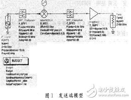
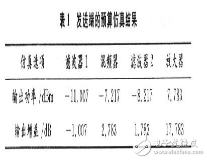
As can be seen from the simulation results in Table 1, the total gain of the entire transmitter is 17.783 dB. The input IF signal is -10 dBm.
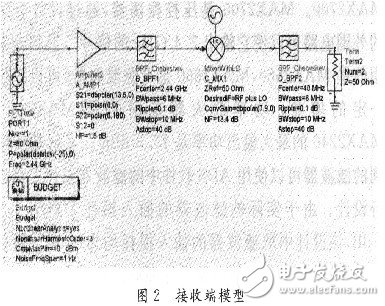
The receiver should consider the gain, noise figure, sensitivity and other factors in the design, which is more complicated than the design of the transmitter. Since the receiving end contains many active devices, the nonlinearity of the active device has a great influence on the entire receiving system. For example, gain compression occurs when only one signal is input, and mutual modulation occurs when more than two signals are input. Wait. In this design, the IF demodulation module also needs a signal size of 8~10 dBm. After analysis, the low noise amplifier uses the MAX2641. The MAX2641 has a gain of 13.5 dB and a noise figure of 1.5 dB. The mixer uses the MAX2682. The MAX2682 has a gain of 7.9 dB and a noise figure of 13.4 dB. The local oscillator is identical to the transmitter. The receiver is modeled using ADS, as shown in Figure 2.
Since the parameters of each module are known, the total noise figure of the system, the third-order intermodulation intercept point, etc. can be obtained through calculation.
The noise figure is defined as the ratio of the system input signal-to-noise power ratio (SNR) i=Pi/N to the output signal-to-noise power ratio (SNR) o=Po/No, which is usually expressed by F. The noise figure characterizes the extent to which the internal noise of the system causes the signal-to-noise ratio to deteriorate after the signal passes through the system. The noise figure is usually expressed in NF (in dB). Cascading based on noise figure:
The total noise figure of the system can be calculated. The total noise figure of the system is viewed from the low-noise amplifier in Figure 3 to the output. The noise figure is also understood to be when the received signal is transmitted by the low-noise amplifier. The output, the degree of deterioration of the signal-to-noise ratio at the receiving end. Using the formula (1), the noise figure of the system is calculated to be F = 2.582 dB and NF = 4.12 dB.
The third-order intercept point IP3 is defined as the point where the third-order intermodulation power reaches the same as the fundamental power. The input power corresponding to this point is represented as IIP3, and the output power corresponding to this point is represented as OIP3. According to the cascade of third-order intermodulation intercept points:
![]()
Available, the total IIP3 of the system = -9.75 dBm. Also in the simulation design environment, the receiver is budget simulated, and the simulation results are shown in Table 2.

From the simulation results in Table 2, it can be seen that the gain of the whole receiving end is 17.205 dB. Assuming that the receiving antenna receives a signal of -30 dBm, the received intermediate frequency signal is -12.795 dBm. The simulated value of the IF signal is slightly lower than the signal required by the IF receiver. This can be used to increase the signal size with a driver amplifier. In addition, the simulation results show that the total noise figure at the receiving end is 4.151 dB, and the calculated result is 4.12 dB. The third-order input intercept point of the simulated receiver is -10.124 dBm, and the calculated value is -9.75 dBm. There is a certain difference in the above results, which is caused by factors such as gain compression. A very important indicator of the receiver is sensitivity, which is defined as the lowest input signal level that the receiver can detect at a given signal-to-noise ratio. Sensitivity is related to the required output signal quality, ie the output signal-to-noise ratio, and to the noise level of the receiver itself. The sensitivity of the receiver can be calculated from:

Assuming that the receiver input satisfies the conjugate match, the noise generated by the noise generated by the source internal resistance Rs to the receiver is its rated output, ie:
![]()
Assuming Ta = 290 K, then NRS = -174 dBm/Hz. So the sensitivity can be expressed as:
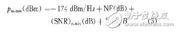
In this design, NF = 4.12 dB, B = 6 MHz, when (SNR) 0, min = 10 dB, calculated by equation (5): pin, min = 92.08 dBm. The strength of the signal received by the receiver varies. The effectiveness of the communication system depends on its dynamic range, ie the range of signal variations that high-performance operation can withstand. The lower limit of the dynamic range is sensitivity, and the upper limit is determined by the maximum acceptable signal distortion. What is considered in this design is the dynamic range of the input of the low noise amplifier. The dynamic range can be obtained from equation (6):
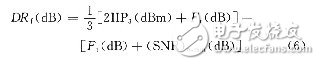
Calculated using equation (6): DRf = 51.58 dB.
Liquid Cooling Servo Motors,Cnc Router Servo Motor,Metal Milling Servo Motor,Ac Spindle Servo Motor
Zhejiang Synmot Electrical Technology Co., Ltd , https://www.synmot-electrical.com