In Xilinx FPGA devices, the global Reset/Reset (GSR) (which can be introduced via the global reset pin) is almost absolutely reliable because it is a signal inside the chip. If all triggers use this global reset signal, the GSR signal will form a high fanout network (interested friends can view it in the synthesis tool). Although it can be synchronized with a user-defined clock in the boot sequence, it is not possible to synchronize it with all clock signals in the design; for example, a Xilinx FPGA may contain multiple DLLs/DCM/ PLL clock processing module, each module can generate multiple clock signals, it is feasible to synchronize the clock signals inside each module. However, it is completely infeasible to synchronize all clock signals - from the distribution of DCM It can be seen that the long-distance wiring in the middle of the interval significantly increases the delay of the high-frequency clock signal, and synchronization cannot naturally be achieved. Thus, as the clock signal frequency becomes higher and higher, the global reset signal begins to become a timing key. Explain as follows:
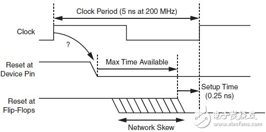
Figure 1 is a timing diagram of the reset signal truncated by the edges of two clock signals
Figure 1 shows the timing diagram of the reset signal that is truncated by the edges of the two clock signals. The first line is the clock signal, the second line is the signal on the device reset pin, and the third line is the reset signal to the reset terminal of the flip-flop. . In order for the flip-flop to be effectively reset, the reset signal should be held for at least one settling time (the resume time of the clock signal) before the valid clock edge arrives. It can be seen that the higher the frequency of the clock signal, the less time is available to allocate the reset signal. Moreover, considering that the global reset signal is often a high fanout network, it is very difficult to meet the demanding timing requirements in this large network. In the design of frequently used asynchronous resets, there is no way to ensure that all flip-flops can be released on the same clock edge, even if there is available time to allocate the reset signal. This can be seen from Figure 2.
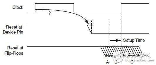
Figure 2 Timing diagram of the reset signal in an asynchronous design
Figure 2 shows the timing diagram of the reset signal in an asynchronous design. It can be seen that the reset signal generated at time A will be generated on the active edge of the first clock signal, and the reset signal generated at time C will be generated on the edge of the second valid clock signal. At time B, it is difficult for the flip-flop to effectively define which reset signal is active, which will result in a metastable state.
With the increase in clock signal frequency and potential clock skew due to increased device size, it is almost impossible to have all flip-flops on the same clock edge. Figure 3 shows the reset timing diagram at high clock frequency.
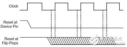
Figure 3 Reset timing at high clock frequency
European Socket Connector
European Socket Connector,30 Position European Socket Connector,Right Angle Male European Socket Connector,Male European Socket Connector
Dongguan Yangyue Metal Technology Co., Ltd , https://www.yyconnector.com